Report an Error


NVIDIA Quadro P620
- Graphics Processor
- GP107
- Cores
- 512
- TMUs
- 32
- ROPs
- 16
- Memory Size
- 2 GB
- Memory Type
- GDDR5
- Bus Width
- 128 bit

GPU
I/O
Recommended Gaming Resolutions:
- 1600x900
- 1920x1080
- 2560x1440
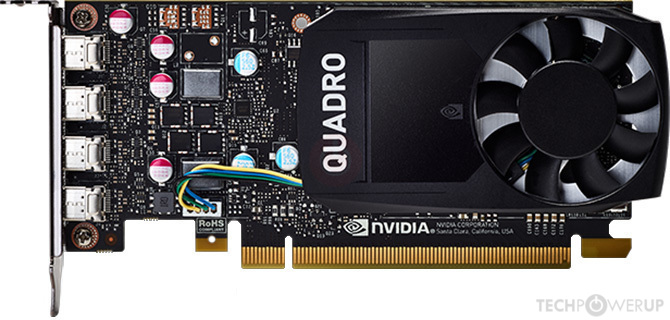
The Quadro P620 was a professional graphics card by NVIDIA, launched on February 1st, 2018. Built on the 14 nm process, and based on the GP107 graphics processor, the card supports DirectX 12. The GP107 graphics processor is an average sized chip with a die area of 132 mm² and 3,300 million transistors. Unlike the fully unlocked GeForce GTX 1050 Ti, which uses the same GPU but has all 768 shaders enabled, NVIDIA has disabled some shading units on the Quadro P620 to reach the product's target shader count. It features 512 shading units, 32 texture mapping units, and 16 ROPs. NVIDIA has paired 2,048 MB GDDR5 memory with the Quadro P620, which are connected using a 128-bit memory interface. The GPU is operating at a frequency of 1266 MHz, which can be boosted up to 1354 MHz, memory is running at 1252 MHz (5 Gbps effective).
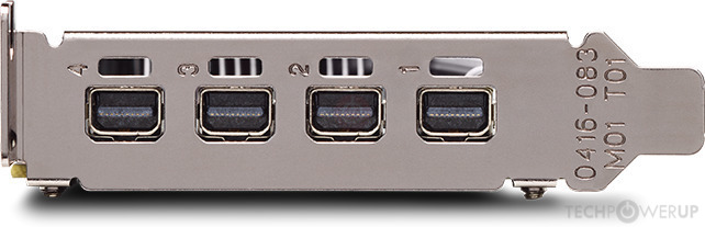
Being a single-slot card, the NVIDIA Quadro P620 does not require any additional power connector, its power draw is rated at 40 W maximum. Display outputs include: 4x mini-DisplayPort 1.4a. Quadro P620 is connected to the rest of the system using a PCI-Express 3.0 x16 interface. The card measures 145 mm in length, 69 mm in width, and features a single-slot cooling solution.
Being a single-slot card, the NVIDIA Quadro P620 does not require any additional power connector, its power draw is rated at 40 W maximum. Display outputs include: 4x mini-DisplayPort 1.4a. Quadro P620 is connected to the rest of the system using a PCI-Express 3.0 x16 interface. The card measures 145 mm in length, 69 mm in width, and features a single-slot cooling solution.
Graphics Processor
Graphics Card
- Release Date
- Feb 1st, 2018
- Generation
-
Quadro Pascal
(Px200)
- Predecessor
- Quadro Maxwell
- Successor
- Quadro Volta
- Production
- End-of-life
- Bus Interface
- PCIe 3.0 x16
Relative Performance
Based on TPU review data: "Performance Summary" at 1920x1080, 4K for 2080 Ti and faster.
Performance estimated based on architecture, shader count and clocks.
Clock Speeds
- Base Clock
- 1266 MHz
- Boost Clock
- 1354 MHz
- Memory Clock
-
1252 MHz
5 Gbps effective
Memory
- Memory Size
- 2 GB
- Memory Type
- GDDR5
- Memory Bus
- 128 bit
- Bandwidth
- 80.13 GB/s
Render Config
- Shading Units
- 512
- TMUs
- 32
- ROPs
- 16
- SM Count
- 4
- L1 Cache
- 48 KB (per SM)
- L2 Cache
- 1024 KB
Theoretical Performance
- Pixel Rate
- 21.66 GPixel/s
- Texture Rate
- 43.33 GTexel/s
- FP16 (half)
- 21.66 GFLOPS (1:64)
- FP32 (float)
- 1,386 GFLOPS
- FP64 (double)
- 43.33 GFLOPS (1:32)
Board Design
- Slot Width
- Single-slot
- Length
- 145 mm
5.7 inches
- Width
- 69 mm
2.7 inches
- TDP
- 40 W
- Suggested PSU
- 200 W
- Outputs
- 4x mini-DisplayPort 1.4a
- Power Connectors
- None
- Board Number
- PG212 SKU 505
Graphics Features
- DirectX
- 12 (12_1)
- OpenGL
- 4.6
- OpenCL
- 3.0
- Vulkan
- 1.3
- CUDA
- 6.1
- Shader Model
- 6.7
GP107 GPU Notes
| NVENC: 6th Gen NVDEC: 3rd Gen PureVideo HD: VP8 VDPAU: Feature Set H |
Retail boards based on this design (1)
| Name | GPU Clock | Boost Clock | Memory Clock | Other Changes |
|---|---|---|---|---|
| 1266 MHz | 1354 MHz | 1252 MHz |

May 8th, 2024 18:53 EDT
change timezone
Latest GPU Drivers
New Forum Posts
- Post your Cinebench R23 Score (2952)
- Flash VBIOS to turn RX 580 2048SP into RX 570 (17)
- im new to throttelstop and i think i messed it up by copying others any hints would be very much aprreciated (15)
- What's a good option for a digital touchless thermometer? (9)
- Does anyone here overclock their video cards? Is it really worth it? (72)
- Your way of cooling your PC? (35)
- TPU's Nostalgic Hardware Club (18503)
- Ubuntu 24.04 LTS released (3)
- POLL: Can you see the difference past 60fps (gaming/other) (58)
- not impressed - nvme vs ssd (72)
Popular Reviews
- CHERRY XTRFY M64 Pro Review
- Corsair iCUE Link RX120 RGB 120 mm Fan Review
- Finalmouse UltralightX Review
- Bykski CPU-XPR-C-I CPU Water Block Review - Amazing Value!
- Upcoming Hardware Launches 2023 (Updated Feb 2024)
- Cougar Hotrod Royal Gaming Chair Review
- Meze Audio LIRIC 2nd Generation Closed-Back Headphones Review
- AMD Ryzen 7 7800X3D Review - The Best Gaming CPU
- ASRock NUC BOX-155H (Intel Core Ultra 7 155H) Review
- ASUS Radeon RX 7900 GRE TUF OC Review
Controversial News Posts
- Intel Statement on Stability Issues: "Motherboard Makers to Blame" (261)
- AMD to Redesign Ray Tracing Hardware on RDNA 4 (206)
- Windows 11 Now Officially Adware as Microsoft Embeds Ads in the Start Menu (167)
- NVIDIA to Only Launch the Flagship GeForce RTX 5090 in 2024, Rest of the Series in 2025 (142)
- Sony PlayStation 5 Pro Specifications Confirmed, Console Arrives Before Holidays (119)
- AMD's RDNA 4 GPUs Could Stick with 18 Gbps GDDR6 Memory (114)
- NVIDIA Points Intel Raptor Lake CPU Users to Get Help from Intel Amid System Instability Issues (106)
- AMD Ryzen 9 7900X3D Now at a Mouth-watering $329 (104)