News Posts matching #6 nm

Return to Keyword Browsing

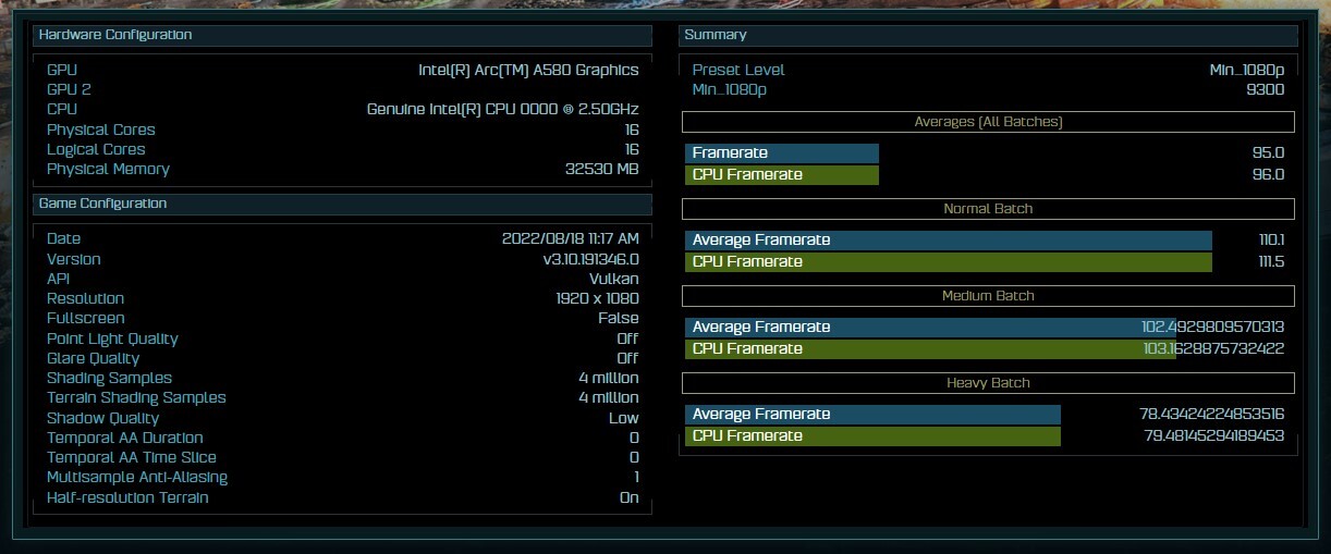
Intel Arc A770 Launched at USD $329, Available from October 12

Intel today announced the pricing for the Arc A770 Limited Edition desktop graphics card, and it is set at USD $329, offering a class of performance comparable to NVIDIA and AMD graphics cards around the $400-range. The A770 is a full-feature DirectX 12 Ultimate-capable graphics cards. The Arc A770 Limited Edition maxes out the 6 nm ACM-G10 silicon, features 32 Xe Cores, 512 XMX matrix processors, and 512 EUs, which work out to 4,096 unified shaders. The card comes with 8 GB or 16 GB of 17.5 Gbps GDDR6 memory across a 256-bit wide memory bus. $329 could be the starting price of the A770 for its 8 GB model. Available from October 12.

Intel Arc A770 Reviews Could Hit Early-October

Reviews of the Intel Arc A770 Limited Edition desktop graphics card could hit the web by October 5, according to a VideoCardz report. These could succeed unboxing articles without performance numbers, on September 30. Press reviews of the A770 publishing on October 5 could mean that retail availability isn't too far behind, and we could hear more about this later today at the IntelON Innovation online event, where the company is widely expected to announce its 13th Gen Core "Raptor Lake" desktop processors. The Arc A770 Limited Edition maxes out the 6 nm ACM-G10 silicon, features 32 Xe Cores, 512 XMX matrix processors, and 512 EUs, which work out to 4,096 unified shaders. The card comes with 8 GB or 16 GB of 17.5 Gbps GDDR6 memory across a 256-bit wide memory bus. Given that Intel is extensively comparing the A770 to the GeForce RTX 3070, one can expect a price competitive to that (around $500).

AMD Ryzen and Athlon 7020 "Mendocino" 6nm Processors Launched for Entry-level Notebooks

AMD today launched the Ryzen 7020 and Athlon 7020 lines of entry-level mobile processors that pack a unique combination of AMD processor, graphics, and I/O technologies that promise a superior experience and battery-life in the entry-level notebook segment that's usually forsaken by processor manufacturers. Based on the 6 nm "Mendocino" monolithic silicon, these SoC pack a 4-core/8-thread CPU based on an enhanced version of the "Zen 2" microarchitecture; an entry-level iGPU based on the latest RDNA2 graphics architecture, with modern display I/O and media-acceleration features; and a modern I/O that includes support for LPDDR5 memory. Processors in the series offer TDP in the range of 8 to 15 W, making them "U-segment" chips but in "H-segment" form-factors. AMD is promising battery-life of up to 12 hours on the full charge.

The 6 nm "Mendocino" silicon packs a single "Zen 2" CCX with four CPU cores, each with 512 KB of dedicated L2 cache, and 4 MB of shared L3 cache. Infinity Fabric connects it with the iGPU, which AMD markets as Radeon 610M. This iGPU packs two RDNA2 compute units (128 stream processors). AMD feels this is enough for everyday computing, web-browsing, and online videos. Its display engine is contemporary, with support for modern notebook display types; while the media engine offers hardware-accelerated decode for H.265 (HEVC), H.264, and AV1, among several older video formats. There are several platform features that Windows 11 can take advantage of, including modern standby, wake-on-voice, including Cortana and Alexa support; Microsoft Ink, and Microsoft Modern Device power-management. Its hardware security features include Pluton, and secure bio channel, making the chips fully capable of running Windows 11 in a commercial environment.

AMD Ryzen 6000 "Rembrandt" Makes it to Mini PCs, Spotted in Upcoming ASUS PN53

The Ryzen 6000-series processors are exclusively-mobile, meant for notebooks and tablets, but is already making its way across several other form-factors, including handheld game consoles, and now desktops, as mini-PCs. Based on the 6 nm "Rembrandt" silicon, Ryzen 6000 combines an up to 8-core/16-thread "Zen 3+" CPU, with an iGPU based on the RDNA2 graphics architecture, with up to 12 compute units; and an exclusively DDR5/LPDDR5 memory interface making for a powerful mobile processor. At least three upcoming ASUS PN53-series mini-PCs powered by "Rembrandt" have surfaced in pre-order online store listings.

Among the three "Rembrandt" powered ASUS PN53 mini-PCs are the ASUS PN53-S9022MD, ASUS PN53-S7021MD, and ASUS PN53-S5020MD. The PN53-S9022MD leads the pack, with a Ryzen 9 6900HX processor (8C/16T, up to 4.90 GHz, 12-CU iGPU, 45 W TDP), 16 GB of DDR5-4800 memory, and 512 GB NVMe SSD; all priced at 1,100€. The ASUS PN53-S7021MD is positioned a notch below, with a Ryzen 7 6800H (8C/16T, up to 4.70 GHz, 12-CU iGPU, 45 W TDP), and otherwise same specs; priced at 1,000€. The ASUS PN53-S5020MD is the most affordable of the lot, powered by a Ryzen 5 6600H (6C/12T, up to 4.50 GHz, 6-CU iGPU, 45 W TDP), 8 GB of DDR5-4800 memory, and 256 GB NVMe storage. This one is going for 840€.

ASRock Arc A750 Challenger Graphics Card Pictured

Here's the first picture of a custom-design Intel Arc A750 "Alchemist" graphics card, in this case, an ASRock Arc A750 Challenger. ASRock showed the card off at its Tokyo Game Show 2022 booth. The strictly 2-slot thick card appears to have a fairly well-endowed aluminium fin-stack cooling solution featuring a pair of large 100 mm fans. Its cooling solution uses two aluminium fin-stacks skewered by a number of copper heat pipes. The card draws power from two 8-pin PCIe power connectors, and features some illumination in the way of an illuminated Arc logo.

The Arc A750 is based on the same 6 nm "DG2-512" silicon as the A770 Limited Edition—which looks increasingly like an Intel-exclusive that will only be sold in its reference design. While the A770 maxes out the chip with all 32 Xe Cores being enabled (512 EUs, or 4,096 unified shaders), the A750 gets 28 Xe Cores (448 EUs, or 3,584 unified shaders). It also gets 8 GB of 16 Gbps GDDR6 memory across a 256-bit wide memory interface (512 GB/s bandwidth), 448 XMX units (accelerates AI and features like XeSS), and 28 RT units. The reference engine clock of the A750 is set at 2.05 GHz, although it's likely that the ASRock Challenger is a factory-overclocked card.

AMD RDNA3 Radeon RX 7000 Flagship GPU PCB Sketched

Here's the very first sketch of an AMD RDNA3 Radeon RX 7000-series flagship graphics card with the "Navi 31" chip in the middle. This will be AMD's first chiplet-based GPU built on a philosophy similar to that of the Ryzen desktop and EPYC server processors. The main number crunching machinery that benefits the most from the latest foundry process, will be built on 5 nm logic chiplets (up to two of these on the "Navi 31," one of these on the "Navi 32"), while the components that don't really benefit from the latest process, such as the memory controllers, display/media accelerators, etc., will be disintegrated into chiplets built on a slightly older node, such as 6 nm. This way AMD gets to maximize its 5 nm allocation at TSMC, which it has to share among not just the logic tiles of RDNA3 GPUs, but also its "Zen 4" processors.

The top-dog "Navi 31" silicon is expected to feature a 384-bit wide GDDR6 memory interface, which is why you see 12 memory chips surrounding the GPU package. AMD is expected to deploy fast 19-21 Gbps class GDDR6 memory chips, as well as double-down on the Infinity Cache technology. The package looks like a GPU die surrounded by HBM stacks, but those are actually the memory/display chiplets. If this PCB is from an AMD reference design, it could be the biggest hint that AMD isn't switching over to the 12+4 pin ATX 12HPWR connector just yet, and could stick with three 8-pin PCIe connectors for power, just like the current RX 6950 XT. USB-C with DisplayPort passthrough could prominently feature with RDNA3 graphics cards, besides standard DisplayPort and HDMI connectors.

AMD EPYC "Genoa" Zen 4 Product Stack Leaked

With its recent announcement of the Ryzen 7000 desktop processors, the action now shifts to the server, with AMD preparing a wide launch of its EPYC "Genoa" and "Bergamo" processors this year. Powered by the "Zen 4" microarchitecture, and contemporary I/O that includes PCI-Express Gen 5, CXL, and DDR5, these processors dial the CPU core-counts per socket up to 96 in case of "Genoa," and up to 128 in case of "Bergamo." The EPYC "Genoa" series represents the main trunk of the company's server processor lineup, with various internal configurations targeting specific use-cases.

The 96 cores are spread twelve 5 nm 8-core CCDs, each with a high-bandwidth Infinity Fabric path to the sIOD (server I/O die), which is very likely built on the 6 nm node. Lower core-count models can be built either by lowering the CCD count (ensuring more cores/CCD), or by reducing the number of cores/CCD and keeping the CCD-count constant, to yield more bandwidth/core. The leaked product-stack table below shows several of these sub-classes of "Genoa" and "Bergamo," classified by use-cases. The leaked slide also details the nomenclature AMD is using with its new processors. The leaked roadmap also mentions the upcoming "Genoa-X" processor for HPC and cloud-compute uses, which features the 3D Vertical Cache technology.

AMD Ryzen 7000X3D Series Reveal by CES 2023?

We already know that AMD is working on a variant of the "Zen 4" CPU complex die (CCD) featuring 3D Vertical Cache (3DV-cache) memory, through company roadmaps, and AMD even confirmed to us that the technology continues to be a part of the client roadmap of the company. We're now getting news that the first Ryzen 7000X3D ("Zen 4" with 3DV cache) processors could be unveiled by the 2023 International CES (January next year). It appears like while the conventional Ryzen 7000 series beats the 12th Gen Core "Alder Lake" at gaming, it might trade blows with the 13th Gen "Raptor Lake," and AMD will count on the 3DV cache technology to give it a competitive edge.

Greymon55, a reliable source with AMD leaks, hints at the possibility of three 7000X3D-series SKUs: the Ryzen 7 7800X3D (8-core/16-thread) positioned above the 7700X; the Ryzen 9 7900X3D (12-core/24-thread), and the Ryzen 9 7950X3D (16-core/32-thread). Older reports suggest the 3DV cache on these processors will be a generation more advanced to keep sync with the on-die L3 cache of the "Zen 4" CCD, and the L3D (the die on which the 3DV cache is located), will likely be built on the 6 nm process.

AMD "Zen 4" Dies, Transistor-Counts, Cache Sizes and Latencies Detailed

As we await technical documents from AMD detailing its new "Zen 4" microarchitecture, particularly the all-important CPU core Front-End and Branch Prediction units that have contributed two-thirds of the 13% IPC gain over the previous-generation "Zen 3" core, the tech enthusiast community is already decoding images from the Ryzen 7000 series launch presentation. "Skyjuice" presented the first annotation of the "Zen 4" core, revealing its large branch-prediction unit, enlarged micro-op cache, TLB, load/store unit, and dual-pumped 256-bit FPU that enables AVX-512 support. A quarter of the core's die-area is also taken up by the 1 MB dedicated L2 cache.

Chiakokhua (aka Retired Engineer) posted a table detailing the various caches and their latencies, comparing it with those of the "Zen 3" core. As AMD's Mark Papermaster revealed in the Ryzen 7000 launch event, the company has enlarged the micro-op cache of the core from 4 K entries to 6.75 K entries. The L1I and L1D caches remain 32 KB in size, each; while the L2 cache has doubled in size. The enlargement of the L2 cache has slightly increased latency, from 12 cycles to 14. Latency of the shared L3 cache is also up, from 46 cycles to 50 cycles. The reorder buffer (ROB) in the dispatch stage has been enlarged from 256 entries to 320 entries. The L1 branch target buffer (BTB) has increased in size from 1 KB to 1.5 KB.

AMD Ready with Zen 4 3DV Cache Chiplet, Expects to Repeat 5800X3D Magic Versus Raptor Lake

AMD is allegedly ready with a working "Zen 4" chiplet that has stacked 3D Vertical Cache (3DV cache) memory, which supplements the on-die L3 cache, and is found to massively improve gaming performance. "Moore's Law is Dead" reports that the Zen 4 + 3DV Cache chiplet will be used with various Ryzen 7000X3D SKUs, as well as special EPYC "Genoa" SKUs.

The 3DV Cache deployed with the "Zen 4" chiplet is a second-generation to the one on the "Zen 3 + 3DV cache" chiplet, and AMD has worked on a number of bandwidth and latency improvements, so it performs in-sync with the generationally-faster on-die L3 cache of the "Zen 4" chiplet. Unlike the CCD below it that's built on TSMC N5 (5 nm EUV), the L3D (the stacked die with the 3DV cache) is possibly be built on an older node, such as N6 (6 nm), since it only contains a slab of memory and doesn't warrant N5. "Moore's Law is Dead" reports that AMD expects to repeat the magic of the 5800X3D when it comes to gaming performance, and expects Ryzen 7000X3D processors to dominate Intel's 13th Gen "Raptor Lake" processors. This was echoed by another reliable source, greymon55.

Intel Data-Center GPU Flex Series "Arctic Sound-M" Launched: Visual Processing, Media, and Inference top Applications

Intel today launched its Arctic Sound M line of data-center GPUs. These are not positioned as HPC processors like the "Ponte Vecchio," but GPUs targeting cloud-compute providers, with their main applications being in the realm of visual processing, media, and AI inferencing. Their most interesting aspect has to be the silicon, which are the same 6 nm "ACM-G11" and "ACM-G10" chips powering the Arc "Alchemist" client graphics cards, based on the Xe-HPG architecture. Even more interesting is their typical board power values, ranging between 75 W to 150 W. The cards are built in the PCI-Express add-on card form-factor, with their cooling solutions optimized for rack airflow.

The marketing name for these cards is simply Intel Data Center GPU Flex, with two models being offered: The Data Center GPU Flex-140, and Flex-170. The Flex-170 is a full-sized add-on card based on the larger ACM-G10 silicon, which has 32 Xe Cores (4,096 unified shaders), whereas the Flex-140, interestingly, is a low-profile dual-GPU card with two smaller ACM-G11 chips that each has 8 Xe Cores (1,024 unified shaders). The two chips appear to be sharing a PCIe bridge chip in the renders. Both models come with four Xe Media Engines that pack AV1 encode hardware-acceleration, XMX AI acceleration, real-time ray tracing, and GDDR6 memory.

TSMC (Not Intel) Makes the Vast Majority of Logic Tiles on Intel "Meteor Lake" MCM

Intel's next-generation "Meteor Lake" processor is the first mass-production client processor to embody the company's IDM 2.0 manufacturing strategy—one of building processors with multiple logic tiles interconnected with Foveros and a base-tile (essentially an interposer). Each tile is built on a silicon fabrication process most suitable to it, so that the most advanced node could be reserved for the component that benefits from it the most. For example, while you need the SIMD components of the iGPU to be built on an advanced low-power node, you don't need its display controller and media engine to, and these could be relegated to a tile built on a less advanced node. This way Intel is able to maximize its use of wafers for the most advanced nodes in a graded fashion.

Japanese tech publication PC Watch has annotated the "Meteor Lake" SoC, and points out that the vast majority of the chip's tiles and logic die-area is manufactured on TSMC nodes. The MCM consists of four logic tiles—the CPU tile, the Graphics tile, the SoC tile, and the I/O tile. The four sit on a base tile that facilitates extreme-density microscopic wiring interconnecting the logic tiles. The base tile is built on the 22 nm HKMG silicon fabrication node. This tile lacks any logic, and only serves to interconnect the tiles. Intel has an active 22 nm node, and decided it has the right density for the job.

Intel Arc A580 Hits AotS Benchmark Database, Roughly Matches RTX 3050

Intel Arc A580 is an upcoming entry-mainstream desktop graphics card based on the Xe-HPG "Alchemist" graphics architecture, and positioned between the A380 and A750. Based on the larger 6 nm DG2-512 silicon than the one powering the A380, the A580 is endowed with 16 Xe Cores, or double the SIMD muscle of the A380, with 2,048 unified shaders. The card enjoys 8 GB of GDDR6 memory across a 128-bit bus, which at 16 Gbps data-rate produces 256 GB/s bandwidth.

A leaked Ashes of the Singularity benchmark database entry reveals that the A580 scores roughly 95 FPS at 1080p on average, with 110 FPS in the normal batch, around 102 FPS in the medium batch, and around 78 FPS in the heavy batch. The benchmark used the Vulkan API, and an unknown 16-thread Intel processor with 32 GB of memory. These scores put the A580 roughly at par with the GeForce RTX 3050 "Ampere" in this test, which would make it a reasonable solution for playing popular online games at 1080p with medium-high settings, or AAA games at medium settings.

Off-season Offsets Wafer Pricing Increase, 1Q22 Foundry Output Value Up 8.2% QoQ, Says TrendForce

According to TrendForce research, although demand for consumer electronics remains weak, structural growth demand in the semiconductor industry including for servers, high-performance computing, automotive, and industrial equipment has not flagged, becoming a key driver for medium and long term foundry growth. At the same time, due to robust wafer production at higher pricing in 1Q22, quarterly output value hit a new high for the 11th consecutive quarter, reaching US$31.96 billion, 8.2% QoQ, marginally less than the previous quarter. In terms of ranking, the biggest change is Nexchip surpassed Tower at the ninth position.

TSMC's across the board wafer hikes in 4Q21 on batches primarily produced in 1Q22 coupled with sustained strong demand for high-performance computing and better foreign currency exchange rates pushed TSMC's 1Q22 revenue to $17.53 billion, up 11.3% QoQ. Quarterly revenue growth by node was generally around 10% and the 7/6 nm and 16/12 nm processes posted the highest growth rate due to small expansions in production. The only instance of revenue decline came at the 5/4 nm process due to Apple's iPhone 13 entering the off season for production stocking.

Intel Arc A380 Desktop Graphics Card Launched in China at $153 (equivalent)

Intel officially launched the Arc A380 "Alchemist" entry-mainstream desktop graphics card in China, priced at RMB ¥1,030, including VAT, which roughly converts to USD $153. The Arc A380 "Alchemist" is based on the Xe-HPG graphics architecture, and the smaller DG2-128 (ACM-G11) silicon, which is built on the TSMC N6 (6 nm) silicon fabrication process.

The A380 desktop GPU is endowed with 8 Xe Cores, or 128 EU (execution units), which work out to 1,024 unified shaders. The chip features a 96-bit wide GDDR6 memory interface, running 6 GB of memory. Despite these hardware specs, you get full DirectX 12 Ultimate capability, including ray tracing, and the XeSS performance enhancement. There are also several content-creation accelerators, including Intel XMX, and AV1 hardware-encode capabilities.

AMD Ryzen 3 7320U Surfaces, Possibly the "Mendocino" SoC

One of AMD's big announcements this fall has been its entry-level "Mendocino" Ryzen 3 mobile processor, which enables the company to compete with Intel's latest-generation Pentium Gold-powered notebooks by combining older-generation IP with the latest I/O and fabrication node. The chip has possibly surfaced on the UserBenchmark database, as the Ryzen 3 7320U processor.

Built on the TSMC N6 (6 nm) silicon fabrication process, the "Mendocino" chip features a 4-core/8-thread CPU based on the older "Zen 2" microarchitecture. This CPU is a single CCX with four "Zen 2" cores sharing a 4 MB L3 cache. It features an iGPU based on the latest RDNA2 graphics architecture, but with just two compute units (128 stream processors). The chip also features a single-channel DDR5 memory interface, and a PCI-Express Gen 3 interface with four PCIe 3.0 general-purpose lanes, besides some USB and display outputs.

AMD EPYC "Bergamo" 128-core Processor Based on Same SP5 Socket as "Genoa"

AMD is launching two distinct classes of next-generation enterprise processors, the 4th Generation EPYC "Genoa" with CPU core-counts up to 96-core/192-thread; and the new EPYC "Bergamo" with a massive 128-core/256-thread compute density. Pictures of the "Genoa" MCM are already out in the wild, revealing twelve "Zen 4" CCDs built on 5 nm, and a new-generation sIOD (I/O die) that's very likely built on 6 nm. The fiberglass substrate of "Genoa" already looks crowded with twelve chiplets, making us wonder if AMD needed a larger package for "Bergamo." Turns out, it doesn't.

In its latest Corporate presentation, AMD reiterated that "Bergamo" will be based on the same SP5 (LGA-6096) package as "Genoa." This would mean that the company either made room for more CCDs, or the CCDs themselves are larger in size. AMD states that "Bergamo" CCDs are based on the "Zen 4c" microarchitecture. Details about "Zen 4c" are scarce, but from what we gather, it is a cloud-optimized variant of "Zen 4" probably with the entire ISA of "Zen 4," and power characteristics suited for high-density cloud environments. These chiplets are built on the same TSMC N5 (5 nm EUV) process as the regular "Zen 4" CCDs.

AMD Unveils 5 nm Ryzen 7000 "Zen 4" Desktop Processors & AM5 DDR5 Platform

AMD today unveiled its next-generation Ryzen 7000 desktop processors, based on the Socket AM5 desktop platform. The new Ryzen 7000 series processors introduce the new "Zen 4" microarchitecture, with the company claiming a 15% single-threaded uplift over "Zen 3" (16-core/32-thread Zen 4 processor prototype compared to a Ryzen 9 5950X). Other key specs about the architecture put out by AMD include a doubling in per-core L2 cache to 1 MB, up from 512 KB on all older versions of "Zen." The Ryzen 7000 desktop CPUs will boost to frequencies above 5.5 GHz. Based on the way AMD has worded their claims, it seems that the "+15%" number includes IPC gains, plus gains from higher clocks, plus what the DDR4 to DDR5 transition achieves. With Zen 4, AMD is introducing a new instruction set for AI compute acceleration. The transition to the LGA1718 Socket AM5 allows AMD to use next-generation I/O, including DDR5 memory, and PCI-Express Gen 5, both for the graphics card, and the M.2 NVMe slot attached to the CPU socket.

Much like Ryzen 3000 "Matisse," and Ryzen 5000 "Vermeer," the Ryzen 7000 "Raphael" desktop processor is a multi-chip module with up to two "Zen 4" CCDs (CPU core dies), and one I/O controller die. The CCDs are built on the 5 nm silicon fabrication process, while the I/O die is built on the 6 nm process, a significant upgrade from previous-generation I/O dies that were built on 12 nm. The leap to 5 nm for the CCD enables AMD to cram up to 16 "Zen 4" cores per socket, all of which are "performance" cores. The "Zen 4" CPU core is larger, on account of more number-crunching machinery to achieve the IPC increase and new instruction-sets, as well as the larger per-core L2 cache. The cIOD packs a pleasant surprise—an iGPU based on the RDNA2 graphics architecture! Now most Ryzen 7000 processors will pack integrated graphics, just like Intel Core desktop processors.

AMD MI300 Compute Accelerator Allegedly Features Eight Logic Dies

AMD's next-generation MI300 compute accelerator is expected to significantly scale up the logic density, according to a rumor by Moore's Law is Dead. Based on the CDNA3 compute architecture, the MI300 will be a monstrous large multi-chip module with as many as 8 logic dies (compute dies), each with its dedicated HBM3 stack. The compute dies (logic dies), will be 3D-stacked on top of I/O dies that pack the memory controllers, and the interconnect that performs the inter-die, and inter-package communication.

The report even goes on to mention that the compute die at the top level of the stack will be built on TSMC N5 (5 nm) silicon fabrication process, while the I/O die below will be TSMC N6 (6 nm). At this point it's not known if AMD will use the package to wire the logic stacks to the memory stacks, or whether it will take the pricier route of using a silicon interposer, but the report supports the interposer theory—that an all-encompassing interposer seats all eight compute dies, all four I/O dies (each with two compute dies), and the eight HBM3 stacks. An interposer is a silicon die that facilitates high density microscopic wiring between two dies on a package, which are otherwise not possible through large package substrate wiring.

BIOSTAR and XFX Release Radeon RX 6400 Graphics Cards

AMD Radeon board partners BIOSTAR and XFX today released their custom-design RX 6400 graphics cards, in what could be a sign that board partners are allowed to quietly release the entry-level GPU. The BIOSTAR Radeon RX 6400 Gaming is a full-height graphics card with a simple aluminium mono-block fan-heatsink, and a lack of any additional power connectors. The XFX Radeon RX 6400 SWFT 105, on the other hand, is a low-profile, single-slot graphics card that may find appeal among the SFF crowd. It appears to be using an aluminium channel-type cooler with a 40-50 mm blower. The RX 6400 is carved out from the 6 nm "Navi 23" silicon by enabling 12 out of 16 RDNA2 compute units (768 stream processors), and comes with 4 GB of GDDR6 memory across the chip's 64-bit wide memory interface. We're hearing that at reference specs, the RX 6400 has a typical graphics power (TGP) of just 53 W, which is how it's able to make do without any power connectors.

PowerColor Radeon RX 6650 XT Hellhound Specs Sheet Hints at Clock Speed Increases Over RX 6600 XT

A leaked specifications sheet of the upcoming PowerColor Radeon RX 6650 XT Hellhound custom-design graphics card, seen by VideoCards, sheds light on AMD's play at carving out the RX 6650 XT. It involves dialing up the engine clocks (GPU clock speed), and memory bandwidth. At this point it is not known if the RX 6650 XT is based on a refined variant of the "Navi 23" silicon, possibly leveraging the TSMC N6 (6 nm) process, or if it's just a case of AMD dialing up clock speeds while pushing up the typical board power, on existing 7 nm (TSMC N7) process.

The RX 6650 XT Hellhound comes with about 4.3% increase in game clocks in its default "OC mode" BIOS, and about 3.7% increase in maximum boost clocks, up from 2593 MHz to 2689 MHz. The "Silent mode" BIOS of the RX 6650 XT Hellhound offers better clock speeds than the "OC mode" BIOS of the RX 6600 XT Hellhound, at 2410 MHz game, 2635 MHz boost, compared to 2382 MHz game, 2593 MHz boost. The other big surprise is memory clocks, with AMD possibly using 17.5 Gbps GDDR6 memory speeds, compared to 16 Gbps on the RX 6600 XT. This results in a 9.4% increase in memory bandwidth. The RX 6600 XT Hellhound uses a single 8-pin PCIe power connector, for an input capacity of 225 W (including the PCIe slot power), which is sufficient for the card's 160 W typical board power. The TBP of the RX 6650 XT Hellhound is not known, but given that its specs sheet still shows single 8-pin, it has to be under 225 W.

ASRock Radeon RX 6400 Challenger Pictured

It looks like launch of the entry-level Radeon RX 6400 desktop graphics card is just around the corner, with pictures of custom-design cards surfacing. The RX 6400 Challenger by ASRock, pictured below, features a simple aluminium monoblock fan-heatsink, and lacks any power connectors, as the 6 nm "Navi 24" silicon can make do with under 75 W TGP. The RX 6400 is armed with 768 stream processors across 12 RDNA2 compute units, and a 64-bit wide GDDR6 memory interface, holding 4 GB of memory. The SKU is expected to formally launch on April 20.

"Navi 31" RDNA3 Sees AMD Double Down on Chiplets: As Many as 7

Way back in January 2021, we heard a spectacular rumor about "Navi 31," the next-generation big GPU by AMD, being the company's first logic-MCM GPU (a GPU with more than one logic die). The company has a legacy of MCM GPUs, but those have been a single logic die surrounded by memory stacks. The RDNA3 graphics architecture that the "Navi 31" is based on, sees AMD fragment the logic die into smaller chiplets, with the goal of ensuring that only those specific components that benefit from the TSMC N5 node (6 nm), such as the number crunching machinery, are built on the node, while ancillary components, such as memory controllers, display controllers, or even media accelerators, are confined to chiplets built on an older node, such as the TSMC N6 (6 nm). AMD had taken this approach with its EPYC and Ryzen processors, where the chiplets with the CPU cores got the better node, and the other logic components got an older one.

Greymon55 predicts an interesting division of labor on the "Navi 31" MCM. Apparently, the number-crunching machinery is spread across two GCD (Graphics Complex Dies?). These dies pack the Shader Engines with their RDNA3 compute units (CU), Command Processor, Geometry Processor, Asynchronous Compute Engines (ACEs), Rendering Backends, etc. These are things that can benefit from the advanced 5 nm node, enabling AMD to the CUs at higher engine clocks. There's also sound logic behind building a big GPU with two such GCDs instead of a single large GCD, as smaller GPUs can be made with a single such GCD (exactly why we have two 8-core chiplets making up a 16-core Ryzen processors, and the one of these being used to create 8-core and 6-core SKUs). The smaller GCD would result in better yields per wafer, and minimize the need for separate wafer orders for a larger die (such as in the case of the Navi 21).

Intel Readies Third DG2 "Alchemist" ASIC with 256 EU

Intel's recently announced Arc "Alchemist" line of discrete gaming graphics processors consists of at least five mobile SKUs across the Arc 3, Arc 5, and Arc 7 lines; with desktop SKUs expected later this year. These are based on one of two ASICs—the DG2-128 (ACM-G11) and the DG2-512 (ACM-G10), both built on the TSMC N6 (6 nm) silicon fabrication process. Coelacanth's Dream discovered a third ASIC when digging through Intel Graphics Compiler code on GitHub, referred to as the "ACM-G12."

This silicon has exactly half the amount of number-crunching machinery as the DG2-512, and features 256 execution units (EU), or 16 Xe cores, working out to 2,048 unified shaders—double that of the DG2-128, but half that of the DG2-512. Interestingly, the Arc 5 A550M mobile GPU announced last week has specifications corresponding to this silicon, even though it was announced to be a heavily cut-down DG2-512. Intel probably figures that at some point making A550M GPUs using DG2-512 could mean cutting down perfectly functional silicon, and so it makes sense to manufacture physically smaller dies (more dies per wafer). There are no other known specs of the ACM-G12. It's quite likely given the rest of its alignment with the A550M's specs that it could feature a 128-bit wide GDDR6 memory interface.

AMD RX 6950 XT, RX 6750 XT, and RX 6650 XT Pictured, Launching on May 10

AMD's Radeon RX product stack refresh for Spring-Summer, is reportedly set to launch on May 10, 2022. Here's the first picture of what a reference-design RX 6950 XT flagship, RX 6750 XT, and the mid-range RX 6650 XT, could look like. These reference board designs are essentially identical to the original RX 6000 made-by-AMD (MBA) reference designs, but ditch the two-tone silver+black color-scheme for an all-black scheme with some diamond-cut edges around the fan vents, and some piano-black accents.

At this point it is not known if this refresh sees the Navi 20-series ASICs optically-shrunk to the TSMC N6 (6 nm) silicon fabrication node, or if it's the existing 7 nm ASICs with their total graphics power (TGP) values dialed up to make room for increased engine clocks, and faster 18 Gbps-rated GDDR6 memory chips. It's interesting to see the RX 6750 XT now come with a triple-fan cooler that resembles the RX 6800 (non-XT) cooler in design, if not color. We're not sure if the RX 6650 XT reference design will ever make it to the real-world, or if it's just a concept, and the SKU is an AIB-exclusive (custom-designs only).
Return to Keyword Browsing
May 11th, 2024 14:47 EDT change timezone

New Forum Posts

Popular Reviews

Controversial News Posts