News Posts matching #6 nm

Return to Keyword Browsing

AMD Radeon RX 7000 Series to Include 6nm Optical-Shrinks of RDNA2

AMD's upcoming Radeon RX 7000 series could include GPUs from both the RDNA3 and RDNA2 graphics architectures, according to reliable sources on social media. This theory holds that the company could introduce new 5 nm GPUs based on the new RDNA3 architecture for the higher end, namely the Navi 31 and Navi 32; while giving the current-gen RDNA2 architecture a new lease of life in the lower segments. This isn't, however, a simple rebrand.

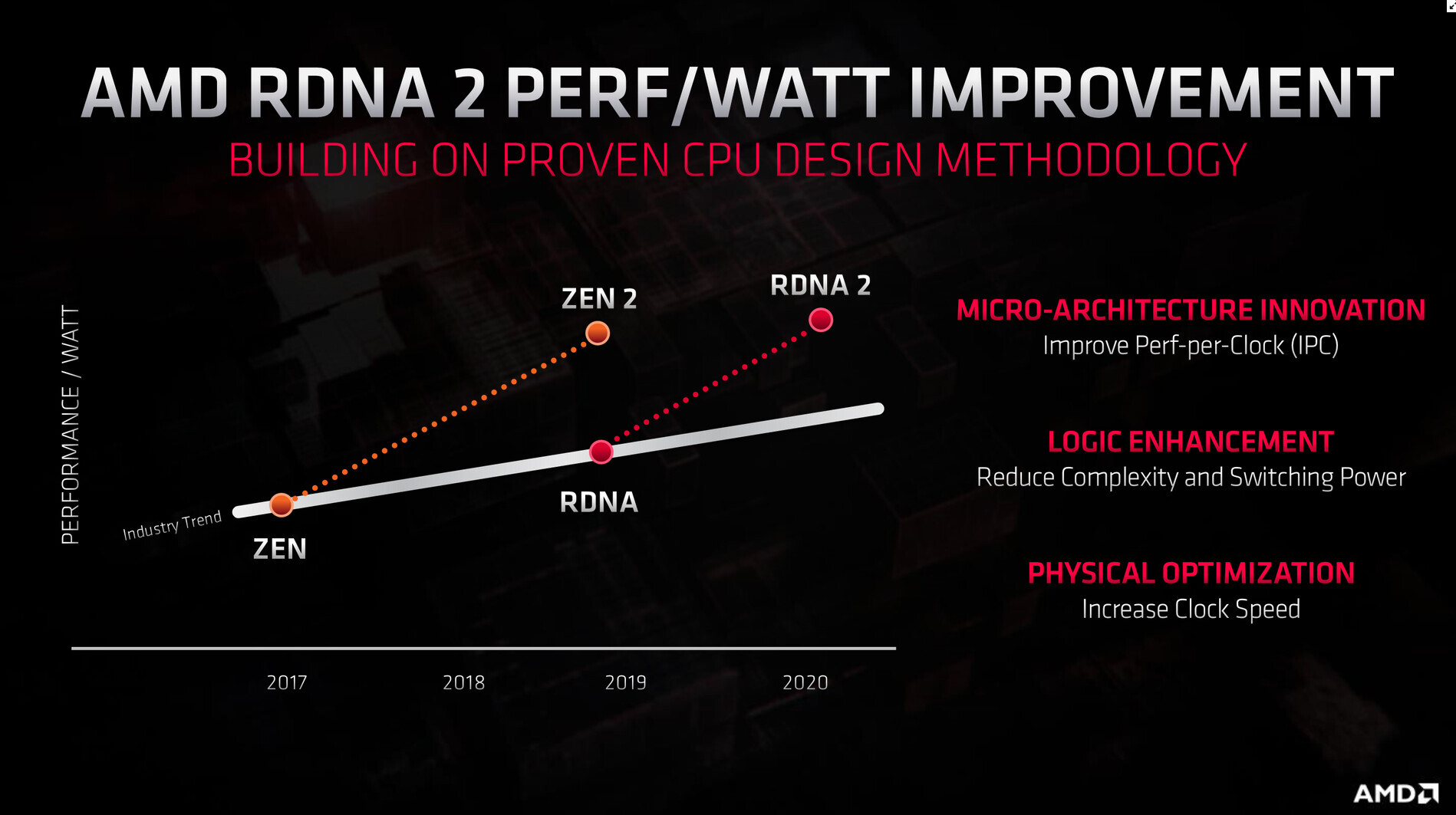
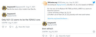
Apparently, some existing Navi 2x series chips will receive an optical shrink to the 6 nm node, in a bid to improve their performance/Watt. Some of the performance/Watt improvement could be used to increase engine clocks. These include the Navi 22, with its 40 RDNA2 compute units and 192-bit GDDR6 memory bus; and the Navi 23, with its 32 RDNA2 compute units and 128-bit GDDR6 memory bus. The updated Navi 22 will power the SKU that succeeds the current RX 6600 XT, while the updated Navi 23 works the lower-mainstream SKU RX x500-class.

Next-Gen AMD Radeon RDNA3 Flagship To Feature 15,360 Stream Processors?

AMD's next generation RDNA3 graphics architecture generation could see a near-quadrupling in raw SIMD muscle over the current RDNA2, according to a spectacular rumor. Apparently, the company will deploy as many as 15,360 stream processors (quadruple that of a Radeon RX 6800), and spread across 60 WGPs (Workgroup Processors), and do away with the compute unit. This is possibly because the RDNA3 compute unit won't be as independent as the ones on the original RDNA or even RDNA2, which begins to see groups of two CUs share common resources.

Another set of rumors suggest that AMD won't play NVIDIA's game of designing GPUs with wide memory bus widths, and instead build on its Infinity Cache technology, by increasing the on-die cache size and bandwidth, while retaining "affordable" discrete memory bus widths, such as 256-bit. As for the chip itself, it's rumored that the top RDNA3 part, the so-called "Navi 31," could feature a multi-chip module design (at least two logic dies), each with 30 WGPs. Each of the two is expected to be built on a next-gen silicon fabrication node that's either TSMC N5 (5 nm), or a special 6 nm node TSMC is designing for AMD. Much like the next-generation "Lovelace" architecture by NVIDIA, AMD's RDNA3 could see the light of the day only in 2022.

AMD Ryzen Embedded V3000 SoCs Based on 6nm Node, Zen 3 Microarchitecture

AMD's next generation Ryzen Embedded V3000 system-on-chips aren't simply "Cezanne" dies sitting on BGA packages, but rather based on a brand new silicon, according to Patrick Schur, a reliable source with leaks. The die will be built on the more advanced 6 nm silicon fabrication node, whilst still being based on the current "Zen 3" microarchitecture. There are several things that set it apart from the APU silicon of the current-generation, making it more relevant for the applications the Ryzen Embedded processor family is originally built for.

Built in the FP7r2 BGA package, the V3000 silicon features an 8-core/16-thread CPU based on the "Zen 3" microarchitecture. There are also an integrated GPU based on the RDNA2 graphics architecture, with up to 12 CUs, a dual-channel DDR5 memory interface, a 20-lane PCI-Express 4.0 root complex, with up to 8 lanes put out for PEG; two USB4 ports, and two 10 GbE PHYs. AMD could design at least three SKUs based on this silicon, spanning TDP bands of 15-30 W and 35-54 W.

Rumor: AMD Rembrandt APUs to Feature Zen3+, RDNA2 Architectures - Up to 12 CUs

A fresh rumor straight from the rumor mill paints AMD's next APU iterations as being updated to the latest and greatest architectures the company has to offer. The rumor comes from ExecutableFix via Twitter, a leaker who has a relatively proven track record on being right regarding upcoming hardware releases. This rumor can lay some credence to others, painting AMD's Ryzen 7000 series as being the first AMD APU-only release since they began their journey with the Zen architecture - it makes sense for the company to integrate their latest architectures in the mobile-geared Rembrandt first, working out some possible interaction quirks that might arise between the two architectures when deployed in the same package.

The leaker further affirms that the Rembrandt APUs will feature up to 12 RDNA2 CUs, which would amount to 768 stream processors on-chip - a marked increase from the current-generation 8 CUs based on the Vega architecture on their Ryzen 4000 mobile series. The leaker also discloses that AMD's Warhol seems to be MIA in recent AMD documentation and planning when it comes to the deployment of Zen3+, and that Rembrandt should be the one to carry that particular architecture refinement through to the 6 nm process. It would seem that AMD's Vega would "finally" see its demise, bringing about some much-needed performance improvements to counter Intel's investments in GPU performance with Xe.

Sony Reportedly Working on Redesigned PS5 SoC on 6 nm for 2022

It's not only graphics cards and CPUs that are best kept on the edge of manufacturing processes; in truth, one could even say that consoles have more to gain from these transitions when it comes to their manufacturers' financial outlooks. This happens because usually, consoles are subsidized by manufacturers in that their actual retail price is lower than manufacturing costs; this works as a way for console players to increase their platforms' attractiveness and user base, so they can then sell them games and subscription services, where the big bucks are actually made. We knew this already, but Microsoft's head of Xbox business development, Lori Wright confirmed it yesterday at the Apple vs Epic Games hearing. Lori Wright is quoted as answering "We don't; we sell the consoles at a loss" when asked whether Microsoft does or does not turn a profit on Xbox Series S | X hardware sales.

Considering the similarities between the Xbox Series X and PS5's SoC, it's very likely that Sony doesn't make a profit on console hardware sales either - or if it actually does, it's nothing actually meaningful. This is part of the reason why consoles are usually actually in the forefront of manufacturing processes' advancements, as it's a way for console players to quickly reduce the BoM (Bill of Materials) for their consoles. Since the specifications don't change within a console generation (discounting Pro models, which both companies have taken to launching some years into their generations), they choose to take advantage of process advancements due to the transistor density increases that allow for both lower silicon area for the SoC, and lower power consumption - which sometimes enables them to develop slim versions of their gaming consoles.

ASML Finishes Development of EUV Pellicles for Greater Sub-7nm Yields

ASML has finally finished development of EUV (Extreme Ultra Violet) pellicles to be employed in manufacturing processes that use the most energetic frequency of visible light to etch semiconductors onto wafers. Pellicles have been used for decades in the industry, and they are basically ultra-thin membranes that protect photomasks during the etching process - impeding particles from depositing in the substrate, which could lead to defects at the wafer level for every subsequent patterning that is laid on top of the impurity. Manufacturers such as TSMC have deployed EUV-powered manufacturing processes, but they have had to toil with potentially lower yields and increased costs with wafer analysis so as to reduce chances of defects appearing.

It's been a long time coming for EUV-capable pellicles, because these have different requirements compared to their traditional, non-EUV counterparts. However, once they are available on the market, it's expected that all semiconductor manufacturers with bleeding-edge manufacturing processes integrate them into their production flows. These will allow for better yields, which in turn should reduce overall pricing for the manufacturing processes. As an example, these EUV masks could be deployed on TSMC's 7 nm, 6 nm, 5 nm, and so on and so on. Other players other than ASML are also finishing their pellicle design, so the industry will have multiple options to integrate into their processes.

New Intel DG2 HPG GPU Surface, Could Power a Family of Products

It appears that Intel's DG2 refers to a number of HPG (High Performance Graphics) products within the same family, with rumors surfacing around a possible total of six different graphics products based on the company's latest high performance graphics architecture - and its debut on the high performance discrete market. It's been confirmed that Intel's DG2 products will not be manufactured in-house, via Intel's 10 nm SuperFin technology, but with recourse to foundry partner TSMC's 6 nm fabrication technology.

It seems that DG2 is currently slated for launch based on three different chip configurations: the first is the DG2 512EU, which will power the highest-performance, 4096 shading unit, 8 GB / 16 GB GDDR6 and 192-bit bus graphics card. Another chip is the DG12 384EU, estimated to come in at ~190 mm², available in three different shading unit configurations: 3072 shading units, with an accompanying 6/12 GB of GDDR6 memory and 192-bit bus; 2048 shading units, which reduces allotted memory to 4/8 GB configurations and a 128-bit memory bus; and finally, the further cut-down 1536 shading unit configuration, with a maximum of 4 GB of GDDR6 memory over the same 128-bit bus. The final (current) chip in the DG2 family is the DG2 128EU, with both 128EU and 96EU configurations (1024 and 768 shading units, respectively) carrying 4 GB VRAM over a pretty tight 64-bit bus. We'll see if these leaks actually materialize into final Intel products, and if these design choices are the possible best, considering Intel's technology, so as to assail the two-player party that is the discrete, high performance graphics market.

SiPearl to Manufacture its 72-Core Rhea HPC SoC at TSMC Facilities

SiPearl has this week announced their collaboration with Open-Silicon Research, the India-based entity of OpenFive, to produce the next-generation SoC designed for HPC purposes. SiPearl is a part of the European Processor Initiative (EPI) team and is responsible for designing the SoC itself that is supposed to be a base for the European exascale supercomputer. In the partnership with Open-Silicon Research, SiPearl expects to get a service that will integrate all the IP blocks and help with the tape out of the chip once it is done. There is a deadline set for the year 2023, however, both companies expect the chip to get shipped by Q4 of 2022.

When it comes to details of the SoC, it is called Rhea and it will be a 72-core Arm ISA based processor with Neoverse Zeus cores interconnected by a mesh. There are going to be 68 mesh network L3 cache slices in between all of the cores. All of that will be manufactured using TSMC's 6 nm extreme ultraviolet lithography (EUV) technology for silicon manufacturing. The Rhea SoC design will utilize 2.5D packaging with many IP blocks stitched together and HBM2E memory present on the die. It is unknown exactly what configuration of HBM2E is going to be present. The system will also see support for DDR5 memory and thus enable two-level system memory by combining HBM and DDR. We are excited to see how the final product looks like and now we wait for more updates on the project.

MediaTek Launches 6nm Dimensity 1200 Premium 5G SoC

MediaTek today unveiled its new Dimensity 1200 and Dimensity 1100 5G smartphone chipsets with unrivaled AI, camera and multimedia features for powerful 5G experiences. The addition of the 6 nm Dimensity 1200 and 1100 chipsets to MediaTek's 5G portfolio gives device makers a growing suite of options to design highly capable 5G smartphones with top of the line camera features, graphics, connectivity enhancements and more.

"MediaTek continues to expand its 5G portfolio with highly integrated solutions for a range of devices from the high-end to the mid-tier," said JC Hsu, Corporate Vice President and General Manager of MediaTek's Wireless Communications Business Unit. "Our new Dimensity 1200 stands out with its impressive 200MP camera support and advanced AI capabilities, in addition to its innovative connectivity, display, audio and gaming enhancements."

Intel Courts TSMC 6nm and 3nm Nodes for Future Xe GPU Generations

Intel is rumored to be aligning its future-generation Xe GPU development with TSMC's node development cycle, with the company reportedly negotiating with the Taiwanese foundry for 6 nm and 3 nm allocation for its large Xe GPUs. Intel's first Xe discrete GPUs for the market, however, are reportedly built on the company's own 10 nm+ silicon fabrication process.

While Intel's fascination with TSMC 3 nm is understandable, seeking out TSMC's 6 nm node raises eyebrows. Internally referred to as "N6," the 6 nm silicon fabrication node at TSMC is expected to go live either towards the end of 2020 or early 2021, which is when Intel's 10 nm+ node is expected to pick up volume production, beginning with the company's "Tiger Lake" processors. Perhaps a decision has been made internally to ensure that Xe doesn't eat too much into Intel's own foundry capacities meant for processor manufacturing, and to instead outsource Xe manufacturing to third-party foundries like TSMC and Samsung eventually. Way back in April 2019 it was rumored that Intel was evaluating Samsung as a foundry partner for Xe.

AMD RDNA2 Graphics Architecture Detailed, Offers +50% Perf-per-Watt over RDNA

With its 7 nm RDNA architecture that debuted in July 2019, AMD achieved a nearly 50% gain in performance/Watt over the previous "Vega" architecture. At its 2020 Financial Analyst Day event, AMD made a big disclosure: that its upcoming RDNA2 architecture will offer a similar 50% performance/Watt jump over RDNA. The new RDNA2 graphics architecture is expected to leverage 7 nm+ (7 nm EUV), which offers up to 18% transistor-density increase over 7 nm DUV, among other process-level improvements. AMD could tap into this to increase price-performance by serving up more compute units at existing price-points, running at higher clock speeds.

AMD has two key design goals with RDNA2 that helps it close the feature-set gap with NVIDIA: real-time ray-tracing, and variable-rate shading, both of which have been standardized by Microsoft under DirectX 12 DXR and VRS APIs. AMD announced that RDNA2 will feature dedicated ray-tracing hardware on die. On the software side, the hardware will leverage industry-standard DXR 1.1 API. The company is supplying RDNA2 to next-generation game console manufacturers such as Sony and Microsoft, so it's highly likely that AMD's approach to standardized ray-tracing will have more takers than NVIDIA's RTX ecosystem that tops up DXR feature-sets with its own RTX feature-set.
AMD GPU Architecture Roadmap RDNA2 RDNA3 AMD RDNA2 Efficiency Roadmap AMD RDNA2 Performance per Watt AMD RDNA2 Raytracing

UNISOC Launches Next-Gen 5G SoC T7520 on 6 nm EUV Manufacturing Node

UNISOC, a leading global supplier of mobile communication and IoT chipsets, today officially launched its new-generation 5G SoC mobile platform - T7520. Using cutting-edge process technology, T7520 enables an optimized 5G experience with substantially enhanced AI computing and multimedia imaging processing capabilities while lowering power consumption.

T7520 is UNISOC's second-generation 5G smartphone platform. Built on a 6 nm EUV process technology and empowered by some of the latest design techniques, it offers substantially enhanced performance at a lower level of power consumption than ever.

Samsung Electronics Begins Mass Production at New EUV Manufacturing Line

Samsung Electronics, a world leader in advanced semiconductor technology, today announced that its new cutting-edge semiconductor fabrication line in Hwaseong, Korea, has begun mass production.

The facility, V1, is Samsung's first semiconductor production line dedicated to the extreme ultraviolet (EUV) lithography technology and produces chips using process node of 7 nanometer (nm) and below. The V1 line broke ground in February 2018, and began test wafer production in the second half of 2019. Its first products will be delivered to customers in the first quarter.

Europe Readies its First Prototype of Custom HPC Processor

European Processor Initiative (EPI) is a Europe's project to kickstart a homegrown development of custom processors tailored towards different usage models that the European Union might need. The first task of EPI is to create a custom processor for high-performance computing applications like machine learning, and the chip prototypes are already on their way. The EPI chairman of the board Jean-Marc Denis recently spoke to the Next Platform and confirmed some information regarding the processor design goals and the timeframe of launch.

Supposed to be manufactured on TSMC's 6 nm EUV (TSMC N6 EUV) technology, the EPI processor will tape-out at the end of 2020 or the beginning of 2021, and it is going to be heterogeneous. That means that on its 2.5D die, many different IPs will be present. The processor will use a custom ARM CPU, based on a "Zeus" iteration of Neoverese server core, meant for general-purpose computation tasks like running the OS. When it comes to the special-purpose chips, EPI will incorporate a chip named Titan - a RISC-V based processor that uses vector and tensor processing units to compute AI tasks. The Titan will use every new standard for AI processing, including FP32, FP64, INT8, and bfloat16. The system will use HBM memory allocated to the Titan processor, have DDR5 links for the CPU, and feature PCIe 5.0 for the inner connection.

AMD Designing Zen 4 for 2021, Zen 3 Completes Design Phase, out in 2020

AMD in its 2nd generation EPYC processor launch event announced that it has completed the design phase of its next-generation "Zen 3" CPU microarchitecture, and is currently working on its successor, the "Zen 4." AMD debuted its "Zen 2" microarchitecture with the client-segment 3rd generation Ryzen desktop processor family, it made its enterprise debut with the 2nd generation EPYC. This is the first x86 CPU microarchitecture designed for the 7 nanometer silicon fabrication process, and is being built on a 7 nm DUV (deep ultraviolet) node at TSMC. It brings about double-digit percentage IPC improvements over "Zen+."

The "Zen 3" microarchitecture is designed for the next big process technology change within 7 nm, EUV (extreme ultraviolet), which allows significant increases in transistor densities, and could facilitate big improvements in energy-efficiency that could be leveraged to increase clock-speeds and performance. It could also feature new ISA instruction-sets. With "Zen 3" passing design phase, AMD will work on prototyping and testing it. The first "Zen 3" products could debut in 2020. "Zen 4" is being designed for a different era.

Intel Switches Gears to 7nm Post 10nm, First Node Live in 2021

Intel's semiconductor manufacturing business has had a terrible past 5 years as it struggled to execute its 10 nanometer roadmap forcing the company's processor designers to re-hash the "Skylake" microarchitecture for 5 generations of Core processors, including the upcoming "Comet Lake." Its truly next-generation microarchitecture, codenamed "Ice Lake," which features a new CPU core design called "Sunny Cove," comes out toward the end of 2019, with desktop rollouts expected 2020. It turns out that the 10 nm process it's designed for, will have a rather short reign at Intel's fabs. Speaking at an investor's summit on Wednesday, Intel put out its silicon fabrication roadmap that sees an accelerated roll-out of Intel's own 7 nm process.

When it goes live and fit for mass production some time in 2021, Intel's 7 nm process will be a staggering 3 years behind TSMC, which fired up its 7 nm node in 2018. AMD is already mass-producing CPUs and GPUs on this node. Unlike TSMC, Intel will implement EUV (extreme ultraviolet) lithography straightaway. TSMC began 7 nm with DUV (deep ultraviolet) in 2018, and its EUV node went live in March. Samsung's 7 nm EUV node went up last October. Intel's roadmap doesn't show a leap from its current 10 nm node to 7 nm EUV, though. Intel will refine the 10 nm node to squeeze out energy-efficiency, with a refreshed 10 nm+ node that goes live some time in 2020.

TSMC Expects Most 7nm Customers to Move to 6nm Density

TSMC in its quarterly earnings call expressed confidence in that most of its 7 nm (N7) process production node customers would be looking to make the transition to their 6 nm (N6) process. In fact, the company expects that node to become the biggest target for volume ordering (and thus production) amongst its customers, since the new N6 fabrication technology will bring about a sort of "backwards compatibility" with design tools and semiconductor designs that manufacturers have already invested in for its N7 node, thus allowing for cost savings for its clients.

This is despite TSMC's N6 process being able to take advantage of extreme ultraviolet lithography (EUVL) to lower manufacturing complexity. This lowering is achieved by the fact that less exposures of the silicon are required for multi-patterning - which is needed today as TSMC's N7 uses solely deep ultraviolet (DUV) lithography. Interestingly, TSMC expects other clients to pick up its N7+ manufacturing node that aren't already using their 7nm node - the need to develop new tools and lesser design compatibility between its N7 and N7+ nodes compared no N7 and N6 being the justification. TSMC's N7+ will be the first node to leverage EUV, using up to four EUVL layers, while N6 expands it up to five layers, and the upcoming N5 cranks EUVL up to fourteen (allowing for 14 layers.)

TSMC Unveils 6-nanometer Process

TSMC today announced its 6-nanometer (N6) process, which provides a significant enhancement of its industry-leading N7 technology and offers customers a highly competitive performance-to-cost advantage as well as fast time-to-market with direct migration from N7-based designs. By leveraging the new capabilities in extreme ultraviolet (EUV) lithography gained from the N7+ technology currently in risk production, TSMC's N6 process delivers 18% higher logic density over the N7 process. At the same time, its design rules are fully compatible with TSMC's proven N7 technology, allowing its comprehensive design ecosystem to be reused. As a result, it offers a seamless migration path with a fast design cycle time with very limited engineering resources for customers to achieve the product benefits from the new technology offering.

Scheduled for risk production in the first quarter of 2020, TSMC's N6 technology provides customers with additional cost-effective benefits while extending the industry-leading power and performance from the 7nm family for a broad array of applications, ranging from high-to-mid end mobile, consumer applications, AI, networking, 5G infrastructure, GPU, and high-performance computing.

Samsung Announces Comprehensive Process Roadmap Down to 4 nm

Samsung stands as a technology giant in the industry, with tendrils stretching out towards almost every conceivable area of consumer, prosumer, and professional markets. It is also one of the companies which can actually bring up the fight to Intel when it comes to semiconductor manufacturing, with some analysts predicting the South Korean will dethrone Intel as the top chipmaker in Q2 of this year. Samsung scales from hyper-scale data centers to the internet-of-things, and is set to lead the industry with 8nm, 7nm, 6nm, 5nm, 4nm and 18nm FD-SOI in its newest process technology roadmap. The new Samsung roadmap shows how committed the company is (and the industry with it) towards enabling the highest performance possible from the depleting potential of the silicon medium. The 4 nm "post FinFET" structure process is set to be in risk production by 2020.

This announcement also marks Samsung's reiteration on the usage of EUV (Extreme Ultra Violet) tech towards wafer manufacturing, a technology that has long been hailed as the savior of denser processes, but has been ultimately pushed out of market adoption due to its complexity. Kelvin Low, senior director of foundry marketing at Samsung, said that the "magic number" for productivity (as in, with a sustainable investment/return ratio) with EUV is 1,500 wafers per day. Samsung has already exceeded 1,000 wafers per day and has a high degree of confidence that 1,500 wafers per day is achievable.
Return to Keyword Browsing
May 4th, 2024 10:05 EDT change timezone

New Forum Posts

Popular Reviews

Controversial News Posts