News Posts matching #ASIC

Return to Keyword Browsing

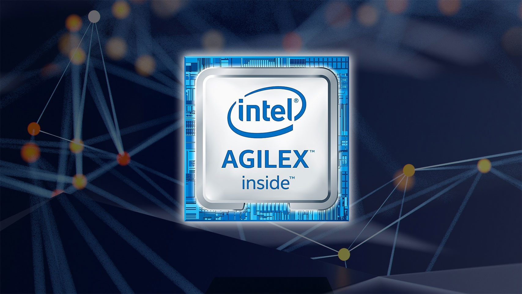
Intel Ships First 10nm Agilex FPGAs

Intel today announced that it has begun shipments of the first Intel Agilex field programmable gate arrays (FPGAs) to early access program customers. Participants in the early access program include Colorado Engineering Inc., Mantaro Networks, Microsoft and Silicom. These customers are using Agilex FPGAs to develop advanced solutions for networking, 5G and accelerated data analytics.

"The Intel Agilex FPGA product family leverages the breadth of Intel innovation and technology leadership, including architecture, packaging, process technology, developer tools and a fast path to power reduction with eASIC technology. These unmatched assets enable new levels of heterogeneous computing, system integration and processor connectivity and will be the first 10nm FPGA to provide cache-coherent and low latency connectivity to Intel Xeon processors with the upcoming Compute Express Link," said Dan McNamara, Intel senior vice president and general manager of the Networking and Custom Logic Group.

Intel Sets Up New Network and Custom-logic Group

In recent conversations with Intel customers, two words kept coming up: disruption and opportunity. Disruption because almost every single executive I talk with has seen business disrupted in one way or another or is worried about keeping up with new technology trends and keeping a competitive edge. And opportunity because when these customers discuss their needs -- be it how to better leverage data, how to modernize their infrastructure for 5G or how to accelerate artificial intelligence (AI) and analytics workloads -- they realize the massive prospects in front of them.

To help our customers capitalize on the opportunities ahead, Intel has created a new organization that combines our network infrastructure organization with our programmable solutions organization under my leadership. This new organization is called the Network and Custom Logic Group.
Both original organizations executed on record design wins and revenues in 2018. Their merger allows Intel to bring maximum value to our customers by delivering unprecedented and seamless access to Intel's broad portfolio of products, from Intel Xeon processors SoC, FPGA, eASIC, full-custom ASIC, software, IP, and systems and solutions across the cloud, enterprise, network, embedded and IoT markets. To that end, FPGA and custom silicon will continue to be important horizontal technologies. And this is just the beginning of a continuum of Custom Logic Portfolio of FPGA, eASIC, and ASIC to support our customers' unique needs throughout their life cycles. No other company in the world can offer that.

Intel Announces New Chief People Officer Sandra Rivera

Intel has announced that Sandra Rivera will take on a new role as the company's chief people officer and executive vice president, reporting to CEO Bob Swan. She will lead the human resources organization and serve as steward of Intel's culture evolution as it transforms to a data-centric company. Previously, Rivera was responsible for the Network Platforms Group, and served as Intel's 5G executive sponsor.

"Sandra is a role model for an Intel that is customer obsessed, collaborative and fearless while firmly grounded in trust, transparency and inclusivity. I am thrilled that Sandra will lead this critical part of our strategy to power a data-centric world," Swan said. "In a company driven by deep, technical talent, Sandra is an excellent technical leader who builds successful businesses by first building great teams. I am confident Sandra, as chief people officer, will help us accelerate our transformation and position our Intel team to play a bigger role in our customers' success."

AMD "Navi" Graphics Card PCB Pictured, uses GDDR6

Pictures of an upcoming AMD Radeon "Navi" graphics card bare PCB made it to the web over the weekend. The picture reveals a fairly long (over 25 cm) board with AMD markings, and a layout that doesn't match with any reference-design PCB AMD launched so far. At the heart of the PCB is a large ASIC pad that appears to be within 5 percent of the size of a "Polaris10" chip. The ASIC is surrounded by eight GDDR6 memory pads. We could guess they're GDDR6 looking at the rectangularity of their pin-layout compared to GDDR5.

The PCB has provision for up to two 8-pin PCIe power inputs, and an 8+1 phase VRM that uses premium components such as rectangular tantalum capacitors, DrMOS, and a high-end VRM controller chip. There's also provision for dual-BIOS. The display I/O completely does away with DVI provisioning, and only includes the likes of DisplayPort, HDMI, and even USB-C based outputs such as VirtualLink. The fan header looks complex, probably offering individual fan-speed control for the card's multi-fan cooling solution that could resemble that of the Radeon VII. Looking purely at the feature-set on offer, and the fact that "Navi" will be more advanced than "Vega 2.0," we expect this card to be fairly powerful, going after the likes of NVIDIA's RTX 2070 and RTX 2060. AMD is expected to unveil this card at the 2019 Computex, this June.

Intel Driving Data-Centric World with New 10nm Intel Agilex FPGA Family

Intel announced today a brand-new product family, the Intel Agilex FPGA. This new family of field programmable gate arrays (FPGA) will provide customized solutions to address the unique data-centric business challenges across embedded, network and data center markets. "The race to solve data-centric problems requires agile and flexible solutions that can move, store and process data efficiently. Intel Agilex FPGAs deliver customized connectivity and acceleration while delivering much needed improvements in performance and power for diverse workloads," said Dan McNamara, Intel senior vice president, Programmable Solutions Group.

Customers need solutions that can aggregate and process increasing amounts of data traffic to enable transformative applications in emerging, data-driven industries like edge computing, networking and cloud. Whether it's through edge analytics for low-latency processing, virtualized network functions to improve performance, or data center acceleration for greater efficiency, Intel Agilex FPGAs are built to deliver customized solutions for applications from the edge to the cloud. Advances in artificial intelligence (AI) analytics at the edge, network and the cloud are compelling hardware systems to cope with evolving standards, support varying AI workloads, and integrate multiple functions. Intel Agilex FPGAs provide the flexibility and agility required to meet these challenges and deliver gains in performance and power.

AMD Brings Back the "XT" Moniker with China-specific Radeon RX 560 XT

Back in the glory days of ATI Radeon, the XT brand extension denoted the better-endowed variant among two or more graphics card models based on the same silicon, such as the Radeon HD 2900 XT. After AMD's takeover, the XT, Pro, XL, and other lesser used extensions such as XTX and All-in-Wonder were retired in favor of numerical variant numbers, beginning with the HD 3870. The company continued to use "XT" and "Pro" internally to differentiate ASIC variants, although those monikers were seldom if not never used in marketing materials. That's about to change. AMD launched its first overtly XT brand-extended product in close to 15 years, with the China-specific Radeon RX 560 XT, but alas, it's a lousy re-brand.

The RX 560 XT is positioned between the RX 560 4 GB and RX 570 4 GB, and is based on the "Polaris 20" or "Polaris 30" silicon (we don't know which). AMD enabled 28 out of 36 NGCUs on this silicon, resulting in 1,792 stream processors, 112 TMUs, and 32 ROPs. The memory is 4 GB across a 256-bit wide memory interface, although the memory clock-speed is dialed down to 6.6 Gbps (211.2 GB/s). What makes the RX 560 XT a re-brand is that AMD launched an SKU with the same exact specifications, called Radeon Pro 570, and there are several odd-ball RX 570-branded cards in the wild with this core-config. There's no reference-design board of the RX 560 XT, and the SKU is entirely in the hands of board partners to come up with custom-designs of their own.

Update: AMD has informed us that the RX 560 XT is based on the 14 nm "Polaris 10" silicon, and not "Polaris 20" or "Polaris 30." Polaris 10 is the first implementation of the "Polaris" architecture.

NVIDIA Readies GeForce GTX 1660 Ti Based on TU116, Sans RTX

It looks like RTX technology won't make it to sub-$250 market segments as the GPUs aren't fast enough to handle real-time raytracing, and it makes little economic sense for NVIDIA to add billions of additional transistors for RT cores. The company is hence carving out a sub-class of "Turing" GPUs under the TU11x ASIC series, which will power new GeForce GTX family SKUs, such as the GeForce GTX 1660 Ti, and other GTX 1000-series SKUs. These chips offer "Turing Shaders," which are basically CUDA cores that have the IPC and clock-speeds rivaling existing "Turing" GPUs, but no RTX capabilities. To sweeten the deal, NVIDIA will equip these cards with GDDR6 memory. These GPUs could still have tensor cores which are needed to accelerate DLSS, a feature highly relevant to this market segment.

The GeForce GTX 1660 Ti will no doubt be slower than the RTX 2060, and be based on a new ASIC codenamed TU116. According to a VideoCardz report, this 12 nm chip packs 1,536 CUDA cores based on the "Turing" architecture, and the same exact memory setup as the RTX 2060, with 6 GB of GDDR6 memory across a 192-bit wide memory interface. The lack of RT cores and a lower CUDA core count could make the TU116 a significantly smaller chip than the TU106, and something NVIDIA can afford to sell at sub-$300 price-points such as $250. The GTX 1060 6 GB is holding the fort for NVIDIA in this segment, besides other GTX 10-series SKUs such as the GTX 1070 occasionally dropping below the $300 mark at retailers' mercy. AMD recently improved its sub-$300 portfolio with the introduction of Radeon RX 590, which convincingly outperforms the GTX 1060 6 GB.

Sapphire Outs an RX 570 Graphics Card with 16GB Memory, But Why?

Sapphire has reportedly developed an odd-ball Radeon RX 570 graphics card, equipped with 16 GB of GDDR5 memory, double the memory amount the SKU is possibly capable of. The card is based on the company's NITRO+ board design common to RX 570 thru RX 590 SKUs, and uses sixteen 8 Gbit GDDR5 memory chips that are piggybacked (i.e. chips on both sides of the PCB). When Chinese tech publication MyDrivers reached out to Sapphire for an explanation behind such a bizarre contraption, the Hong Kong-based AIB partner's response was fascinating.

Sapphire in its response said that they wanted to bolster the card's crypto-currency mining power, and giving the "Polaris 20" GPU additional memory would improve its performance compared to ASIC miners using the Cuckoo Cycle algorithm. This can load up the video memory anywhere between 5.5 GB to 11 GB, and giving the RX 570 16 GB of it was Sapphire's logical next step. Of course Cuckoo Cycle is being defeated time and again by currency curators. This card will be a stopgap for miners until ASIC mining machines with expanded memory come out, or the proof-of-work systems are significantly changed.

AMD Radeon RX 570 and China-specific RX 580 2048SP Based on Exact Same Chip

It's no news that AMD's Radeon RX 570 graphics card is carved out of the same "Polaris 20" silicon as the RX 580, by disabling 4 out of 36 GCN compute units. AMD kicked a controversy recently, when it launched a China-specific Radeon RX 580-branded SKU with the core-configuration of the cheaper RX 570, confusing Chinese consumers. It turns out that this RX 580 2,048 SP SKU is based on the same exact ASIC variant of the "Polaris 20" silicon as the RX 570, with the only difference being device ID.

We watch a lot of GamersNexus content. Our GPU Database curator noticed something interesting in their recent teardown of a Dataland Radeon RX 580 (2,048 SP) graphics card directly imported from China. The unique ASIC sub-variant code etched on the GPU's aluminium reinforcement brace matches that of the RX 570. AMD internally refers to the RX 570 as "Polaris 20 XL," and its ASIC code etched is supposed to be "215-0910052." For the RX 580, the real one, aka "Polaris 20 XTX," the code etched is "215-0910038." Thanks to GamersNexus' high-resolution filming, our curator was able to spot the ASIC code for "Polaris 20 XL" on the Dataland card's GPU. This confirms that AMD merely took an RX 570 and gave it a different device ID to create the RX 580 2,048 SP, leaving consumers to wade through the confusion.

NVIDIA Segregates Turing GPUs; Factory Overclocking Forbidden on the Cheaper Variant

While working on GPU-Z support for NVIDIA's RTX 20-series graphics cards, we noticed something curious. Each GPU model has not one, but two device IDs assigned to it. A device ID is a unique identification that tells Windows which specific device is installed, so it can select and load the relevant driver software. It also tells the driver, which commands to send to the chip, as they vary between generations. Last but not least, the device ID can be used to enable or lock certain features, for example in the professional space. Two device IDs per GPU is very unusual. For example, all GTX 1080 Ti cards, whether reference or custom design, are marked as 1B06. Titan Xp on the other hand, which uses the same physical GPU, is marked as 1B02. NVIDIA has always used just one ID per SKU, no matter if custom-design, reference or Founders Edition.

We reached out to industry sources and confirmed that for Turing, NVIDIA is creating two device IDs per GPU to correspond to two different ASIC codes per GPU model (for example, TU102-300 and TU102-300-A for the RTX 2080 Ti). The Turing -300 variant is designated to be used on cards targeting the MSRP price point, while the 300-A variant is for use on custom-design, overclocked cards. Both are the same physical chip, just separated by binning, and pricing, which means NVIDIA pretests all GPUs and sorts them by properties such as overclocking potential, power efficiency, etc.

GlobalFoundries Puts its 7 nm Program on Hold Indefinitely

GLOBALFOUNDRIES today announced an important step in its transformation, continuing the trajectory launched with the appointment of Tom Caulfield as CEO earlier this year. In line with the strategic direction Caulfield has articulated, GF is reshaping its technology portfolio to intensify its focus on delivering truly differentiated offerings for clients in high-growth markets.

GF is realigning its leading-edge FinFET roadmap to serve the next wave of clients that will adopt the technology in the coming years. The company will shift development resources to make its 14/12nm FinFET platform more relevant to these clients, delivering a range of innovative IP and features including RF, embedded memory, low power and more. To support this transition, GF is putting its 7nm FinFET program on hold indefinitely and restructuring its research and development teams to support its enhanced portfolio initiatives. This will require a workforce reduction, however a significant number of top technologists will be redeployed on 14/12nm FinFET derivatives and other differentiated offerings.

NVIDIA "TU102" RT Core and Tensor Core Counts Revealed

The GeForce RTX 2080 Ti is indeed based on an ASIC codenamed "TU102." NVIDIA was referring to this 775 mm² chip when talking about the 18.5 billion-transistor count in its keynote. The company also provided a breakdown of its various "cores," and a block-diagram. The GPU is still laid out like its predecessors, but each of the 72 streaming multiprocessors (SMs) packs RT cores and Tensor cores in addition to CUDA cores.

The TU102 features six GPCs (graphics processing clusters), which each pack 12 SMs. Each SM packs 64 CUDA cores, 8 Tensor cores, and 1 RT core. Each GPC packs six geometry units. The GPU also packs 288 TMUs and 96 ROPs. The TU102 supports a 384-bit wide GDDR6 memory bus, supporting 14 Gbps memory. There are also two NVLink channels, which NVIDIA plans to later launch as its next-generation multi-GPU technology.

NVIDIA GeForce RTX 2080 Ti TU102 Die-size Revealed

Here are some of the first pictures of NVIDIA's GeForce RTX 2080 Ti ASIC, probably codenamed "TU102." GamersNexus took a ruler to this chip, and discovered that it's one of the biggest non-storage chips in existence. The rectangular die measures 31 mm x 25 mm, or 775 mm². The package has no IHS, but a metal brace along the periphery of the fiberglass substrate distributes mounting pressure from the cooler. NVIDIA is building the "Turing" family of GPUs on TSMC 12 nm FinFET node.

NVIDIA GTX 1080-successor a Rather Hot Chip, Reference Cooler Has Dual-Fans

The GeForce GTX 1080 set high standards for efficiency. Launched as a high-end product that was faster than any other client-segment graphics card at the time, the GTX 1080 made do with just a single 8-pin PCIe power connector, and had a TDP of just 180W. The reference-design PCB, accordingly, has a rather simple VRM setup. The alleged GTX 1080-successor, called either GTX 1180 or GTX 2080 depending on who you ask, could deviate from its ideology of extreme efficiency. There were telltale signs of this departure on the first bare PCB shots.

The PCB pictures revealed preparation for an unusually strong VRM design, given that this is an NVIDIA reference board. It draws power from a combination of 6-pin and 8-pin PCIe power connectors, and features a 10+2 phase setup, with up to 10 vGPU and 2 vMem phases. The size of the pads for the ASIC and no more than 8 memory chips confirmed that the board is meant for the GTX 1080-successor. Adding to the theory of this board being unusually hot is an article by Chinese publication Benchlife.info, which mentions that the reference design (Founders Edition) cooling solution does away with a single lateral blower, and features a strong aluminium fin-stack heatsink ventilated by two top-flow fans (like most custom-design cards). Given that NVIDIA avoided such a design for even big-chip cards such as the GTX 1080 Ti FE or the TITAN V, the GTX 1080-successor is proving to be an interesting card to look forward to. But then what if this is the fabled GTX 1180+ / GTX 2080+, slated for late-September?

NVIDIA Briefs AIC Partners About Next-gen GeForce Series

NVIDIA has reportedly briefed its add-in card (AIC) partners about its upcoming GeForce product family, codenamed "Turing," and bearing a commercial nomenclature of either GeForce 11-series, or GeForce 20-series. This sets in motion a 2-3 month long process of rolling out new graphics cards by board partners, beginning with reference-design "Founders Edition" SKUs, followed by custom-design SKUs. Sources tell Tom's Hardware Germany that AIC partners have began training product development teams. NVIDIA has also released a BoM (bill of materials) to its partners, so aside from the ASIC itself, they could begin the process of sourcing other components for their custom-design products (such as coolers, memory chips, VRM components, connectors, etc.).

The BoM also specifies a timeline for the tentative amount of time it takes for each of the main stages of the product development, leading up to mass-production. It stipulates 11-12 weeks (2-3 months) leading up to mass-production and shipping, which could put product-launch some time in August (assuming the BoM was released some time in May-June). A separate table also provides a fascinating insight to the various stages of development of a custom-design NVIDIA graphics card.

Bitmain Intros Antminer E3 for Ethereum, GPU Prices Could Finally Cool Down

It was only a matter of time before ASICs turned the tide on GPU-accelerated crypto-currency mining. Bitmain announced the Antminer E3, an ASIC miner purpose-built for Ethereum mining. Priced at $800 (or less than the price of an AMD Radeon RX 580 in January), this ASIC draws about 800W of power, and offers a hash-rate of 180 MH/s. To put that into perspective, an RX 580 only has about 30 MH/s, and draws around 200W at typical mining load. Bitmain has begun accepting orders for the Antminer E3, with shipping to commence in July. At its price, no GPU in the market can match the economics of this ASIC, and hence, VGA prices could begin to cool down, and GPU miners could find it hard to hodl on to their overpriced VGAs.

Intel's "Bitcoin Mining Hardware Accelerator" Patent Filling Published

A filed patent by Intel has shed some light on the company's idea to somewhere, along the fuzzy lines of the future, introduce a Bitcoin mining hardware "accelerator" to the market. The application itself, for a "Bitcoin Mining Hardware Accelerator With Optimized Message Digest and Message Scheduler Datapath" was originally submitted in September 2016, so it's not exactly a novel idea. However, the fact that it has just now been published doesn't really mean there hasn't been work behind closed doors at Intel towards development of working silicon of this technology.

In the filing, it appears it's Intel's intent to create a chip that could augment the existing Bitcoin mining process by increasing energy efficiency. As they themselves put it, "Because the software and hardware utilized in Bitcoin mining uses brute force to repeatedly and endlessly perform SHA-256 functions, the process of Bitcoin mining can be very power-intensive and utilize large amounts of hardware space. The embodiments described herein optimize Bitcoin mining operations by reducing the space utilized and power consumed by Bitcoin mining hardware."

AMD Corrects Analyst's Cryptomining Revenue Estimate in Defense of Its Share Value

AMD has gone on to publicly call attention to what it considers to be erroneous information put forward by Susquehanna analyst Christopher Roland. The analyst's report, which prompted the reclassification of AMD and NVIDIA's share targets - and investment ratings. Looking to stem what could translate to lower confidence from investors in its share outlook for the future, AMD has now gone on to clarify that mining revenue actually accounts for single-digit amounts entering the company's coffers, and not the 20% previously mentioned by the analyst.

AMD was dealt a worse hand than NVIDIA on Cristopher Rolland's analysis, since the perceived AMD exposition to a negative downturn on the GPU cryptocurrency mining market (kickstarted by the expected entrance in the market of Ethereum-specific ASICs) was double that of NVIDIA (20% on the former versus 10% on the latter). As such, the company has tried to remind customers, investors, and would-be investors that they appreciate the time and attention that investors continue to pay to Blockchain and cryptocurrency, but "(...) we [AMD] would also like to keep it in perspective with the multiple other growth opportunities ahead for AMD." You can read the AMD statement in full after the break, under the title "The View from Our Corner of the Street".

NVIDIA, AMD to Face Worsening Investment Outlook as Bitmain Preps to Launch Ethereum ASIC

Analyst firm Susquehanna has cut AMD and NVIDIA's share price targets on the wake of confirmed reports on Bitmain's upcoming Ethereum ASIC. There's been talks about such a product for months - and some actual silicon steering as well that might support it. Susquehanna, through analyst Christopher Rolland in a note to clients Monday, cited their travels in Asia as a source of information.

This has brought confirmations that "(...) Bitmain has already developed an ASIC [application-specific integrated circuit] for mining Ethereum, and is readying the supply chain for shipments in 2Q18." And it doesn't seem Bitmain is the only company eyeing the doors of yet another extremely lucrative ASIC mining market: "While Bitmain is likely to be the largest ASIC vendor (currently 70-80% of Bitcoin mining ASICs) and the first to market with this product, we have learned of at least three other companies working on Ethereum ASICs, all at various stages of development."

CTS Labs Posts Some Clarifications on AMD "Zen" Vulnerabilities

CTS-Labs the research group behind the AMD "Zen" CPU vulnerabilities, posted an addendum to its public-release of the whitepaper, in an attempt to dispel some of the criticism in their presentation in the absence of technical details (which they shared with AMD and other big tech firms). In their clarification whitepaper, quoted below, they get into slightly more technical details on each of the four vulnerability classes.

NVIDIA Bracing for a Cryptocurrency Demand Drop

In what could bring cheers to PC gamers, and tears to miners, NVIDIA is reportedly wary of a possible drop in cryptocurrencies through 2018. This directly affects the company, since GPUs are used in mining various cryptocurrencies, which triggered inflation in prices of graphics cards from Q2-2017 to Q1-2018. Over the past couple of weeks, prices of popular high-end GPUs such as the GeForce GTX 1080 Ti have cooled, although not back to their original levels. NVIDIA's manufacturing division, which sub-contracts silicon fabrication to TSMC, is calculating the impact a cryptocurrency slump could have on its supply-chain, and are being conservative with their orders to the foundry. A drop in demand could leave the company with vast amounts of unsold inventories based on an old-generation architecture (Pascal, in the wake of Volta/Ampere), which could result in multi-billion-dollar inventory write-offs. According to a Digitimes report, NVIDIA has placed restrictions on its add-in card (AIC) partners on marketing cryptocurrency mining abilities of their graphics cards, and selling directly to large miners.

In addition to a slump in demand for cryptocurrencies, 2018 could see introduction of purpose-built crypto-mining ASICs that are tailored for popular cryptocurrencies. Purpose-built ASICs tend to be extremely economical for medium-thru-large scale miners, in comparison to GPUs. The third horseman is policy. While several governments around the world have developed an appreciation for blockchain technology for its resilience to tampering, fraud, and data-theft (which could be implemented in safekeeping government- and bank-records); governments are, understandably, anti-cryptocurrency, as it undermines sovereign legal tender issued by central banks, and aids tax-evasion. Several governments through 2017-18 have announced measures to crack down on cryptocurrency mining and use as tender. This has led to a further drop in public interest in cryptocurrencies, as large ICO investors are weary of losing money in a highly volatile market. Close to half the ICOs have failed.

TSMC To Receive Strong Revenue Boost on the Back of Extra ASIC Sales in 2018

TSMC is the world's sole ASIC manufacturer for Bitmain - the world's largest ASIC vendor by far, commanding some 70% of the ASIC market share. DigiTimes is reporting that ASIC manufacturing will be a major part of bridging the 10-15% increase in revenue that TSMC's chairman Morris Chang expects for 2018, which will be mostly fed by high-performance computing (HPC), car-use electronics and Internet of Things (IoT) products.

One other interesting tidbit that DigiTimes is reporting on is that Bitmain might be increasing its ASIC orders from TSMC to bring a new Ethereum ASIC miner to market. Dubbed the F3, reports around the internet have placed these ASICs as leveraging TSMC's 28 nm process in a three-mainboard system. Each mainboard is reported to pack six purpose-built ASIC processors, each paired with 12GB of DDR3 memory. Whether or not this makes sense based on Ethereum's Casper update (moving from a Proof of Work to a Proof of Stake mechanism) remains to be seen. Considering the amount of work and investment that would be required towards the development of an Ethereum ASIC, though (a natively ASIC-resistant algorithm) may very well be an indicator that Casper may be longer off in the horizon than previously thought. Let's hope this is true, though; an Ethereum-geared ASIC, even if short-lived, would certainlydraw demand away from GPUs to these purpose-built systems, and there's been nary a time in the PC world where such an event was as needed as it is today.
Return to Keyword Browsing
May 4th, 2024 14:52 EDT change timezone

New Forum Posts

Popular Reviews

Controversial News Posts