News Posts matching #CDNA2

Return to Keyword Browsing

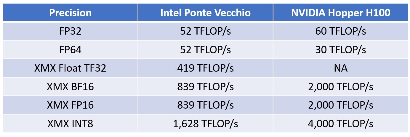
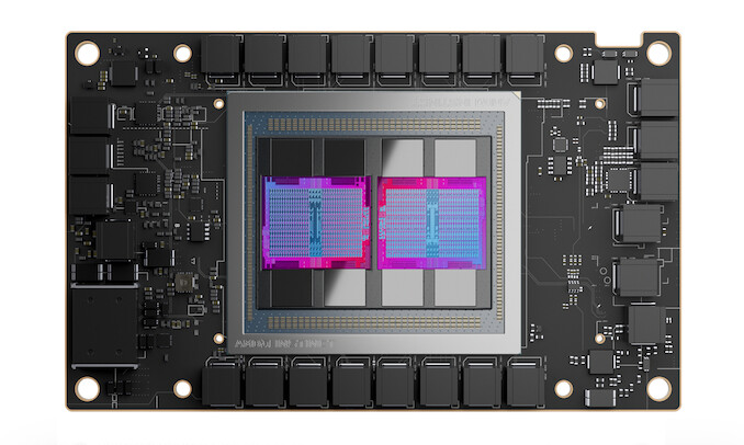
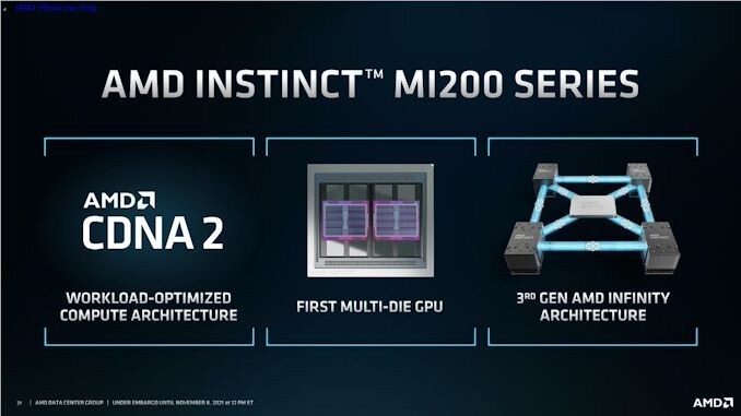
AMD Releases its CDNA2 MI250X "Aldebaran" HPC GPU Block Diagram

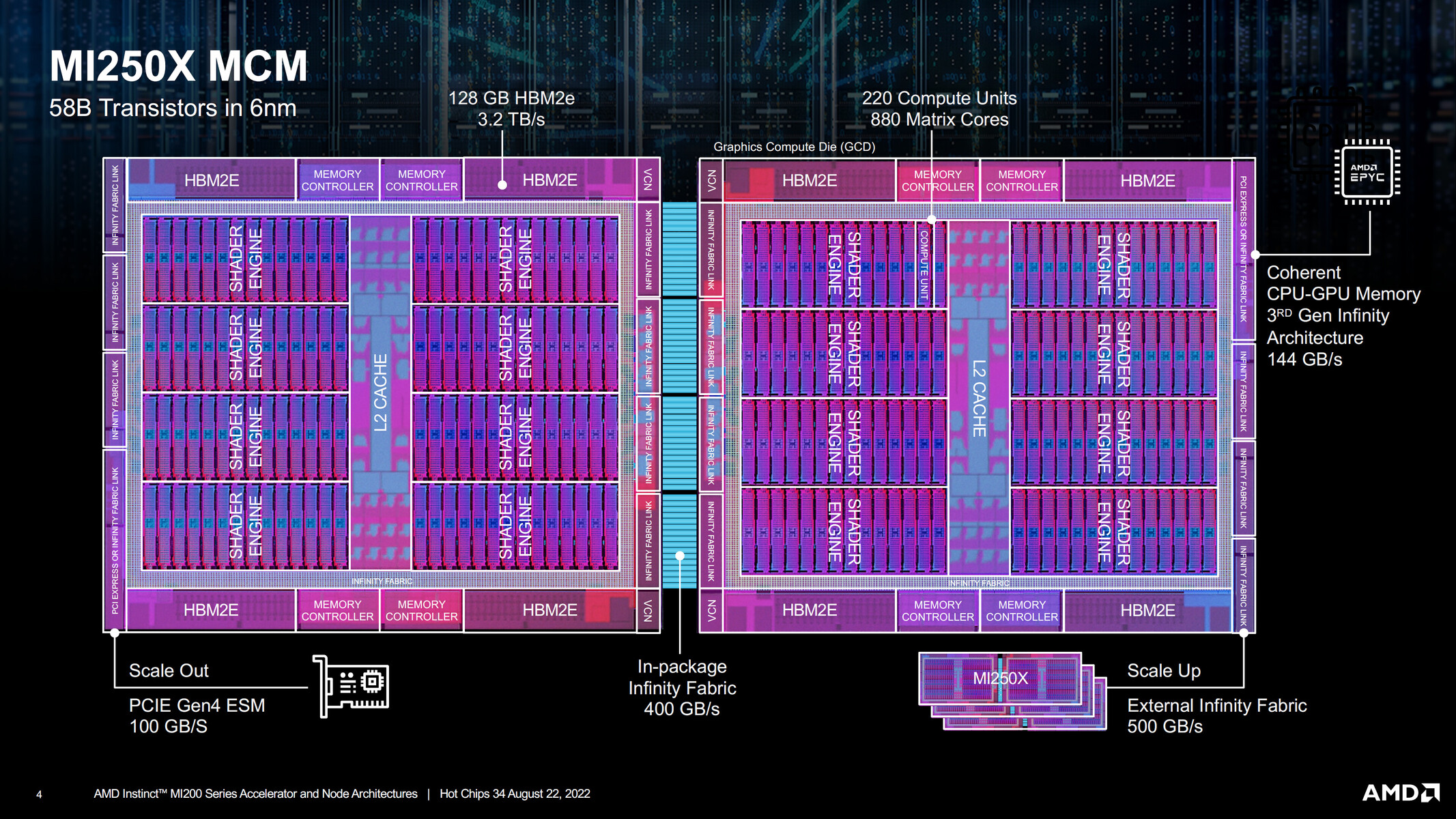
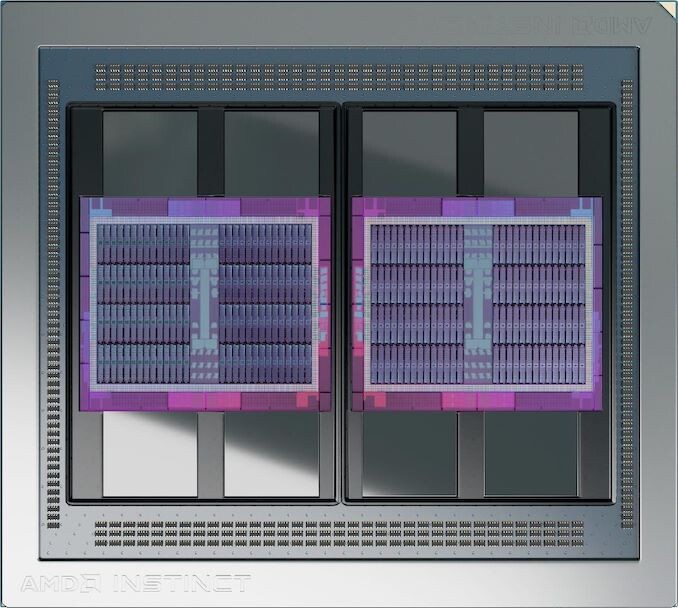
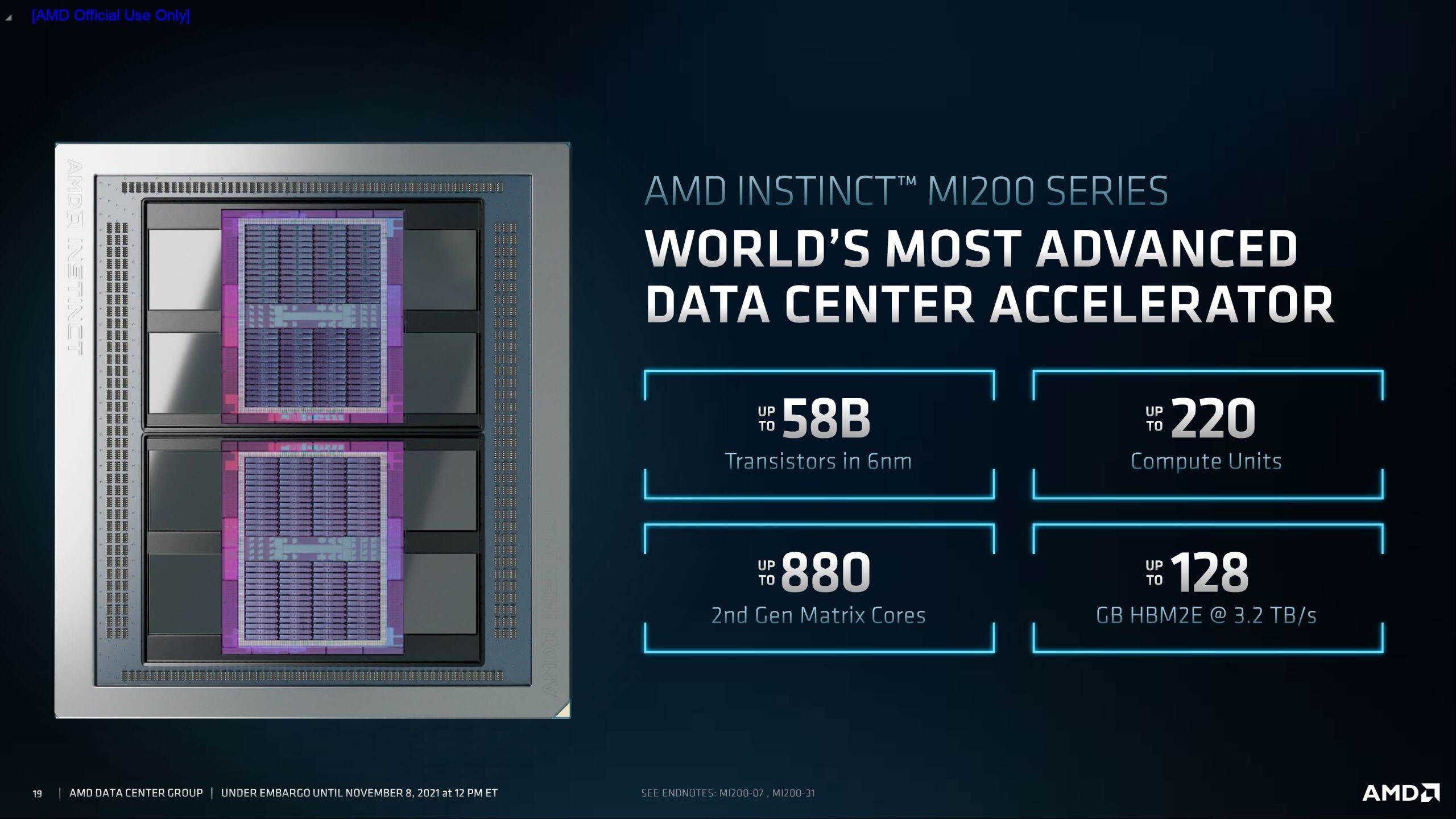
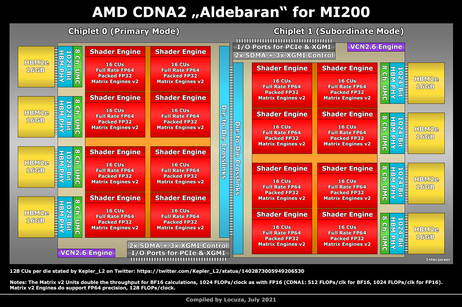
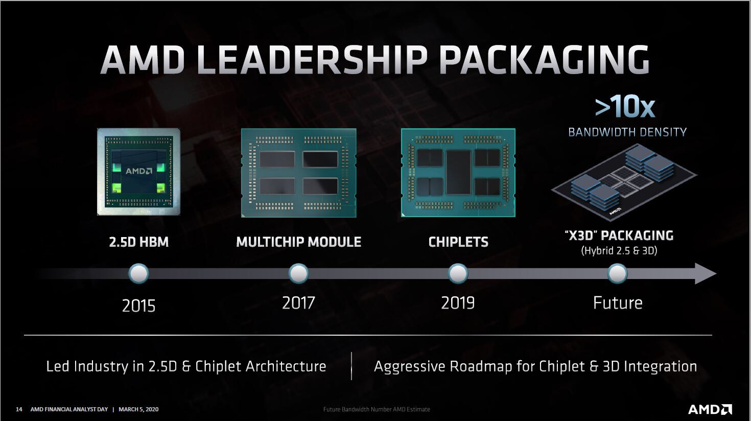
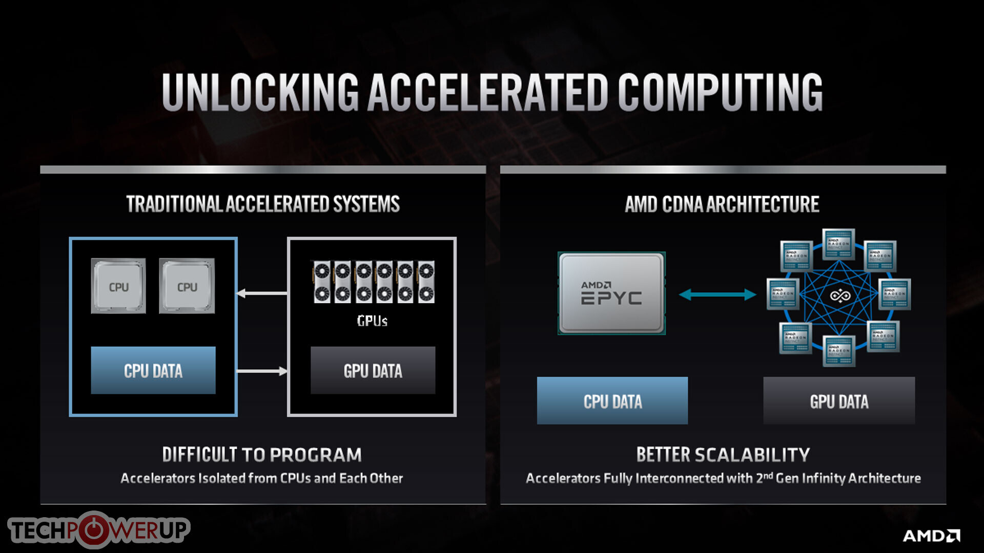
AMD in its HotChips 22 presentation released a block-diagram of its biggest AI-HPC processor, the Instinct MI250X. Based on the CDNA2 compute architecture, at the heart of the MI250X is the "Aldebaran" MCM (multi-chip module). This MCM contains two logic dies (GPU dies), and eight HBM2E stacks, four per GPU die. The two GPU dies are connected by a 400 GB/s Infinity Fabric link. They each have up to 500 GB/s of external Infinity Fabric bandwidth for inter-socket communications; and PCI-Express 4.0 x16 as the host system bus for AIC form-factors. The two GPU dies together make up 58 billion transistors, and are fabricated on the TSMC N6 (6 nm) node.

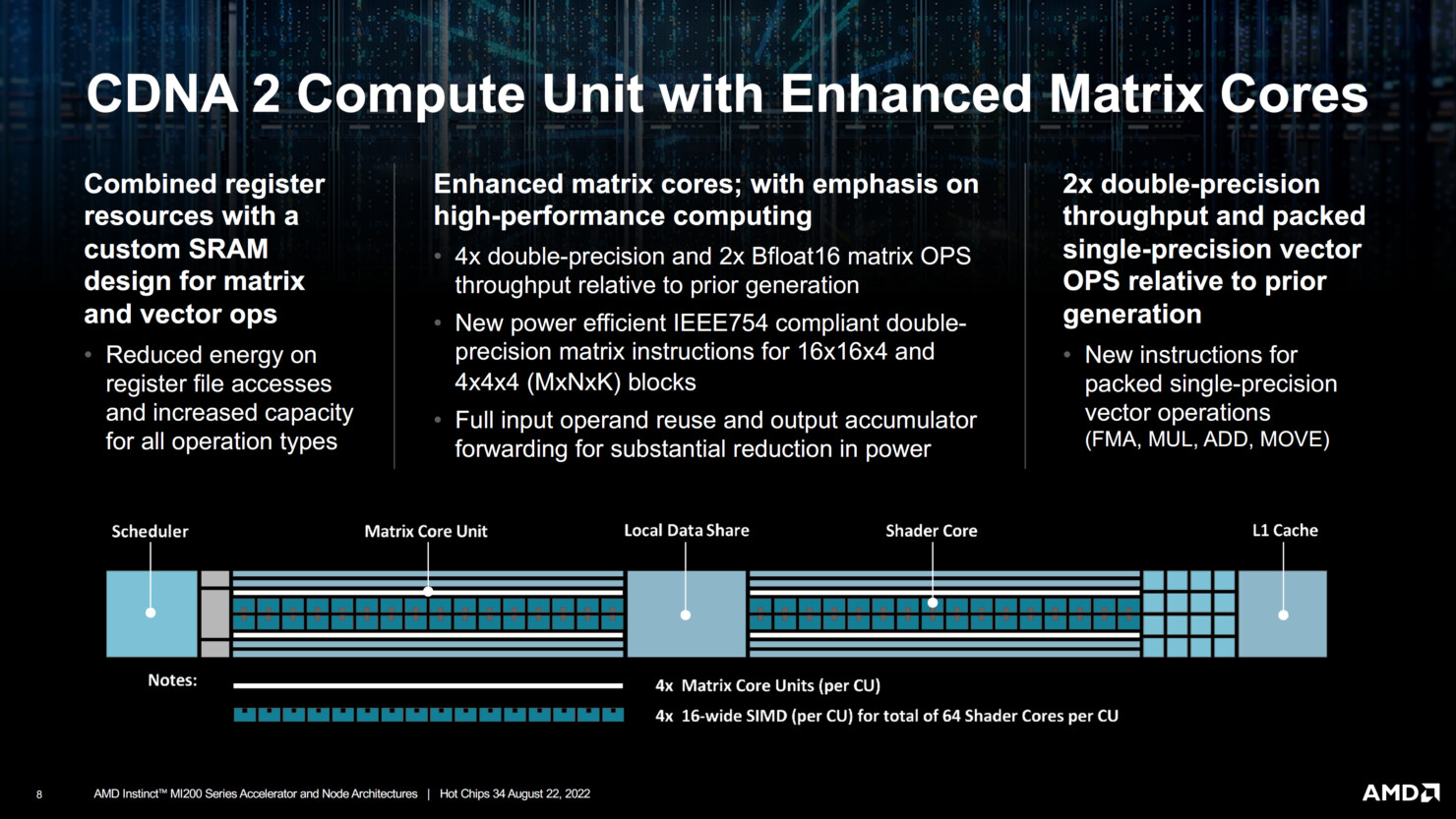
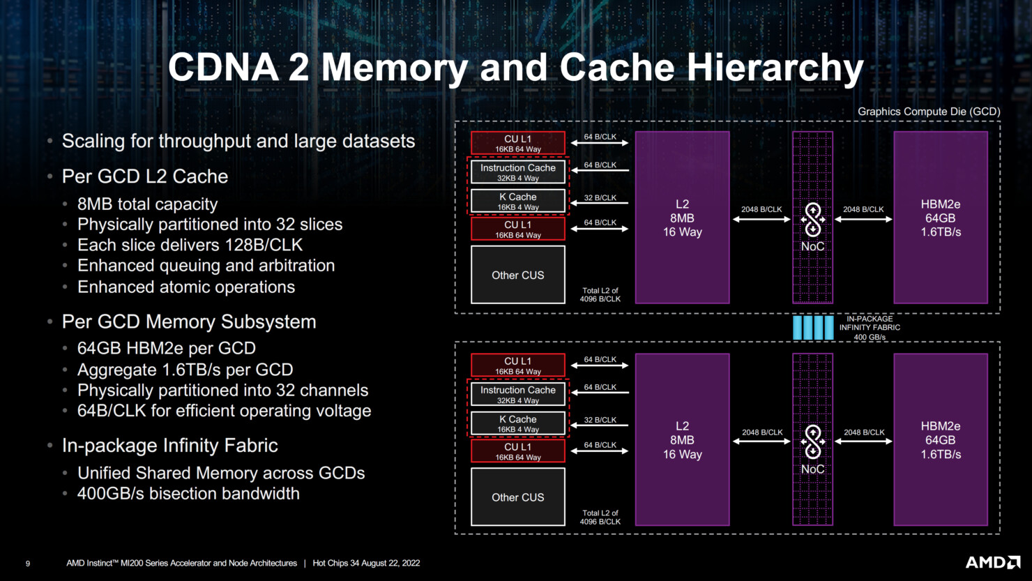
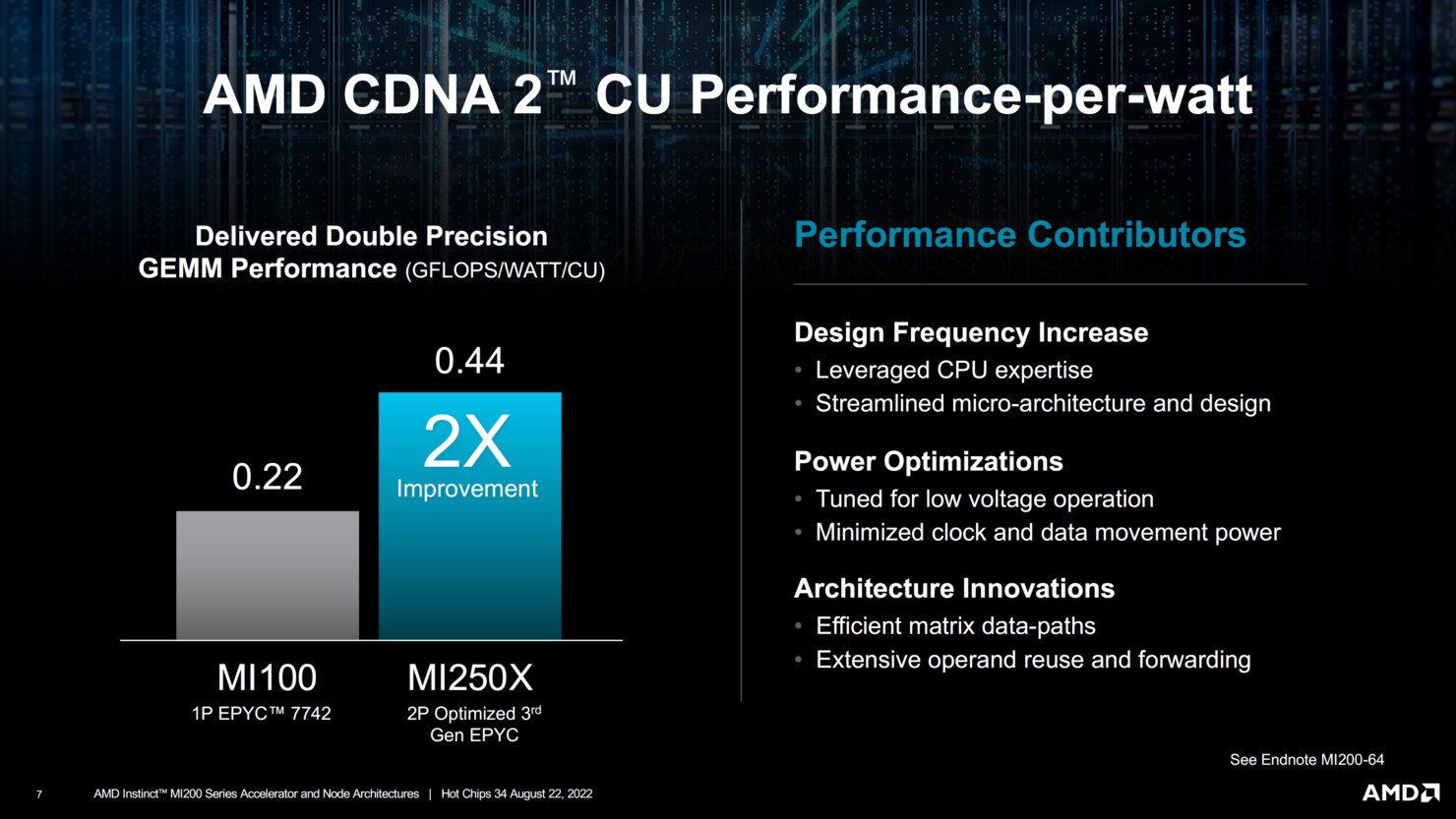
The component hierarchy of each GPU die sees eight Shader Engines share a last-level L2 cache. The eight Shader Engines total 112 Compute Units, or 14 CU per engine. The CDNA2 compute unit contains 64 stream processors making up the Shader Core, and four Matrix Core Units. These are specialized hardware for matrix/tensor math operations. There are hence 7,168 stream processors per GPU die, and 14,336 per package. AMD claims a 100% increase in double-precision compute performance over CDNA (MI100). AMD attributes this to increases in frequencies, efficient data paths, extensive operand reuse and forwarding; and power-optimization enabling those higher clocks. The MI200 is already powering the Frontier supercomputer, and is working for more design wins in the HPC space. The company also dropped a major hint that the MI300, based on CDNA3, will be an APU. It will incorporate GPU dies, core-logic, and CPU CCDs onto a single package, in what is a rival solution to NVIDIA Grace Hopper Superchip.

Intel Claims "Ponte Vecchio" Will Trade Blows with NVIDIA Hopper in Most Compute Workloads

With AMD and NVIDIA launching its next-generation HPC compute architectures, "Hopper" and CDNA2, it began seeming like Intel's ambitious "Ponte Vecchio" accelerator based on the Xe-HP architecture, has missed the time-to-market bus. Intel doesn't think so, and in its Hot Chips 34 presentation, disclosed some of the first detailed performance claims that—at least on paper—put the "Hopper" H100 accelerator's published compute performance numbers to shame. We already had some idea of how Ponte Vecchio would perform this spring, at Intel's ISC'22 presentation, but the company hadn't finalized the product's power and thermal characteristics, which are determined by its clock-speed and boosting behavior. Team blue claims to have gotten over the final development hurdles, and is ready with some big numbers.

Intel claims that in classic FP32 (single-precision) and FP64 (double-precision) floating-point tests, its silicon is highly competitive with the H100 "Hopper," with the company claiming 52 TFLOP/s FP32 for the "Ponte Vecchio," compared to 60 TFLOP/s for the H100; and a significantly higher 52 TFLOP/s FP64 for the "Ponte Vecchio," compared to 30 TFLOP/s for the H100. This has to do with the SIMD units of the Xe-HP architecture all being natively capable of double-precision floating-point operations; whereas NVIDIA's architecture typically relies on FP64-specialized streaming multiprocessors.

AMD Introduces Instinct MI210 Data Center Accelerator for Exascale-class HPC and AI in a PCIe Form-Factor

AMD today announced a new addition to the Instinct MI200 family of accelerators. Officially titled Instinct MI210 accelerator, AMD tries to bring exascale-class technologies to mainstream HPC and AI customers with this model. Based on CDNA2 compute architecture built for heavy HPC and AI workloads, the card features 104 compute units (CUs), totaling 6656 Streaming Processors (SPs). With a peak engine clock of 1700 MHz, the card can output 181 TeraFLOPs of FP16 half-precision peak compute, 22.6 TeraFLOPs peak FP32 single-precision, and 22.6 TFLOPs peak FP62 double-precision compute. For single-precision matrix (FP32) compute, the card can deliver a peak of 45.3 TFLOPs. The INT4/INT8 precision settings provide 181 TOPs, while MI210 can compute the bfloat16 precision format with 181 TeraFLOPs at peak.

The card uses a 4096-bit memory interface connecting 64 GBs of HMB2e to the compute silicon. The total memory bandwidth is 1638.4 GB/s, while memory modules run at a 1.6 GHz frequency. It is important to note that the ECC is supported on the entire chip. AMD provides an Instinct MI210 accelerator as a PCIe solution, based on a PCIe 4.0 standard. The card is rated for a TDP of 300 Watts and is cooled passively. There are three infinity fabric links enabled, and the maximum bandwidth of the infinity fabric link is 100 GB/s. Pricing is unknown; however, availability is March 22nd, which is the immediate launch date.

AMD places this card directly aiming at NVIDIA A100 80 GB accelerator as far as the targeted segment, with emphasis on half-precision and INT4/INT8 heavy applications.

AMD Posts November Investor Presentation

AMD later this month is preparing to address investors as part of a yet-unknown event. The company typically hosts Financial Analyst Day events around Q1-Q2, and goes to the investors with substantial material on the current state of the organization, the products on offer, what's on the horizon, and how it could impact the company's financials. An alleged presentation related to the November 2021 event was leaked to the web. The presentation provides a guided tour of the entire product portfolio of the company, spanning server processors, compute accelerators, consumer graphics, some client processors, and the semi-custom business.

The presentation outlines that the company has so far successfully executed its roadmaps for the client-CPU, server-CPU, graphics, and compute-accelerator segments. In the client CPU segment, it shows a successful execution up to 2021 with the "Zen 3" microarchitecture. In the server space, it mentions successful execution for its EPYC processors up to "Zen 3" with its "Milan" processors, and confirms that its next-generation "Zen 4" microarchitecture, and its sister-architecture, the "Zen 4c," will be built on the 5 nm silicon fabrication node (likely TSMC N5). The presentation also details the recently announced "Milan-X" processor for existing SP3 platforms, which debuts the 3D Vertical Cache technology, bringing up to 96 MB of L3 cache per CCD, and up to 768 MB of L3 cache (804 MB L1+L2+L3 cache) per socket.
Update 10:54 UTC: The presentation can now be found on the AMD Investor Relations website.

TSMC 3 nm To Enter Volume Production in 2022

TSMC will commercialize its N3 (3 nm) EUV silicon fabrication node in 2022, with volume production set to commence in the second half of the year. The company is looking to maximize capacity on its current N5 (5 nm) node, which already serves major customers such as Apple. AMD is expected to utilize N5 allocation going into 2022 as its next-generation "Zen 4" processors are expected to leverage the node to drive up CPU core counts and caches. The company is also utilizing N6 (6 nm) for its CDNA2 compute accelerator logic dies. N5 could also power mobile application processors from several manufacturers.

AMD Details Instinct MI200 Series Compute Accelerator Lineup

AMD today announced the new AMD Instinct MI200 series accelerators, the first exascale-class GPU accelerators. AMD Instinct MI200 series accelerators includes the world's fastest high performance computing (HPC) and artificial intelligence (AI) accelerator,1 the AMD Instinct MI250X.

Built on AMD CDNA 2 architecture, AMD Instinct MI200 series accelerators deliver leading application performance for a broad set of HPC workloads. The AMD Instinct MI250X accelerator provides up to 4.9X better performance than competitive accelerators for double precision (FP64) HPC applications and surpasses 380 teraflops of peak theoretical half-precision (FP16) for AI workloads to enable disruptive approaches in further accelerating data-driven research.

AMD Stock Jumps 10% on Monday, Propelled by Meta (Facebook) Deal

AMD on Monday made several major announcements covering different parts of its enterprise product roadmap. These included the 3rd Gen EPYC "Milan-X" processors with 3D Vertical Cache memory; Instinct MI200 CDNA2 compute accelerators, and announcements related to next-generation "Zen 4" based EPYC "Genoa" and "Bergamo" processors that come with core counts as high as 128. The company's stock rallied up to 12%, closing up 10%, which left many in the tech community scratching their heads. It turns out that the AMD-Meta deal has a profound impact on investors.

Meta, the holding company of Facebook covering all its businesses, aspires to be a major cloud solutions provider on par with Microsoft Azure, AWS, and Google Cloud. The deal could see Meta buying large stocks of AMD processors and compute accelerators to drive its next-gen server infrastructure. Sales of enterprise processors doubled year-over-year for AMD, and EPYC processors now account for 20% of the company's revenues.

AMD Instinct MI200: Dual-GPU Chiplet; CDNA2 Architecture; 128 GB HBM2E

AMD today announced the debut of its 6 nm CDNA2 (Compute-DNA) architecture in the form of the MI200 family. The new, dual-GPU chiplet accelerator aims to lead AMD into a new era of High Performance Computing (HPC) applications, the high margin territory it needs to compete in for continued, sustainable growth. To that end, AMD has further improved on a matured, compute-oriented architecture born with Graphics Core Next (GCN) - and managed to improve performance while reducing total die size compared to its MI100 family.

AMD Accelerated Data Center Event Live Blog

AMD held its Accelerated Data Center Keynote address by CEO Dr Lisa Su today. The company made some big announcements for the enterprise space in this first major series of announcements by AMD after Intel's launch of its Alder Lake 12th Gen Core processors that set the tone for what's to come from Intel in the enterprise space (Xeon "Sapphire Rapids"). First up is the EPYC "Milan-X" line of server processors leveraging 3D Infinity Cache memory, a tripling in L3 cache amount, which the company claims significantly improves performance of memory-intensive applications. This should also give you an idea if any upcoming Ryzen desktop processor based on the refreshed chiplet could live up to its claim of "up to 15% gaming performance boost." The next-generation Instinct MI200 series GPU compute accelerators are equally important as they bring the CDNA2 compute architecture to market, establishing competition to NVIDIA's A-series Tensor Core processors, and Intel's upcoming "Ponte Vecchio" Xe-HPC accelerators.

AMD Readies MI250X Compute Accelerator with 110 CUs and 128 GB HBM2E

AMD is preparing an update to its compute accelerator lineup with the new MI250X. Based on the CDNA2 architecture, and built on existing 7 nm node, the MI250X will be accompanied by a more affordable variant, the MI250. According to leaks put out by ExecutableFix, the MI250X packs a whopping 110 compute units (7,040 stream processors), running at 1.70 GHz. The package features 128 GB of HBM2E memory, and a package TDP of 500 W. As for speculative performance numbers, it is expected to offer double-precision (FP64) throughput of 47.9 TFLOP/s, ditto full-precision (FP32), and 383 TFLOP/s half-precision (FP16 and BFLOAT16). AMD's MI200 "Aldebaran" family of compute accelerators are expected to square off against Intel's "Ponte Vecchio" Xe-HPC, and NVIDIA Hopper H100 accelerators in 2022.

Intel Ponte Vecchio Early Silicon Puts Out 45 TFLOPs FP32 at 1.37 GHz, Already Beats NVIDIA A100 and AMD MI100

Intel in its 2021 Architecture Day presentation put out fine technical details of its Xe HPC Ponte Vecchio accelerator, including some [very] preliminary performance claims for its current A0-silicon-based prototype. The prototype operates at 1.37 GHz, but achieves out at least 45 TFLOPs of FP32 throughput. We calculated the clock speed based on simple math. Intel obtained the 45 TFLOPs number on a machine running a single Ponte Vecchio OAM (single MCM with two stacks), and a Xeon "Sapphire Rapids" CPU. 45 TFLOPs sees the processor already beat the advertised 19.5 TFLOPs of the NVIDIA "Ampere" A100 Tensor Core 40 GB processor. AMD isn't faring any better, with its production Instinct MI100 processor only offering 23.1 TFLOPs FP32.

AMD Stock Breaks $100 Price, Slightly Up from $7 Prior to Zen Breakthrough in 2017

As of 16:11 UTC today (29/07), the AMD stock has broken through the $100 stock-price glass ceiling, and is at $103.91, up 1384% from the $7 stock price in late-2016, prior to the company's competitive breakthrough with the "Zen" architecture. The latest rally comes in the wake of AMD's latest Q2-2021 financial results, where it clocked a 99% growth in YoY revenue. In the call, AMD mentioned that it is on track to maintaining its performance leadership, on the backs of the new "Zen 4" CPU architecture, RDNA3 graphics-, and CDNA2 compute architecture.

AMD Zen 4 and RDNA3 Confirmed for 2022, Zen 3 Refresh

AMD CEO Dr Lisa Su, in the company's Q2-2021 financial results call, confirmed that the company is on-track to launch the Zen 4 CPU microarchitecture and RDNA3 graphics architecture, in 2022. Zen 4 would herald the first major desktop platform change since the original Zen architecture, with the introduction of a new CPU socket, and support for DDR5 memory. The RDNA3 graphics architecture, meanwhile, is expected to nearly triple SIMD resources over the previous generation, and introduce even more fixed-function hardware for raytracing.

In the meantime, AMD is preparing a counter to Intel's 12th Gen Core "Alder Lake-S" processor, in the form of Zen 3 with 3D Vertical Cache, which is also being referred to as the Zen 3+ architecture. These processors feature additional last-level cache, and the company claims a 15% gaming performance uplift, which should help it close the gaming performance gap with Intel, and win on sheer core-count of its big cores. It remains to be seen if Zen 3+ remains on Socket AM4 or if it debuts AM5, as AMD will be under pressure to match "Alder Lake" in platform I/O, which includes DDR5. Dr Su also confirmed that AMD has started shipping the Instinct MI200 "Aldebaran" compute accelerator based on the CDNA2 architecture. AMD's first MCM GPU with two logic dies, "Aldebaran" takes the fight to NVIDIA's top A100 series compute accelerators, and has already scored wins with ongoing HPC/supercomputing projects.

AMD MI200 "Aldebaran" Memory Size of 128GB Per Package Confirmed

The 128 GB per package memory size of AMD's upcoming Instinct MI200 HPC accelerator was confirmed, in a document released by Pawsey SuperComputing Centre, a Perth, Australia-based supercomputing firm that's popular with mineral prospecting companies located there. The company is currently working on Setonix, a 50-petaFLOP supercomputer being put together by HP Enterprise, which combines over 750 next-generation "Aldebaran" GPUs (referenced only as "AMD MI-Next GPUs"); and over 200,000 AMD EPYC "Milan" processor cores (the actual processor package count would be lower, and depend on the various core configs the builder is using).

The Pawsey document mentions 128 GB as the per-GPU memory. This corresponds with the rumored per-package memory of "Aldebaran." Recently imagined by Locuza_, an enthusiast who specializes in annotation of logic silicon dies, "Aldebaran" is a multi-chip module of two logic dies and eight HBM2E stacks. Each of the two logic dies, or chiplets, has 8,192 CDNA2 stream processors that add up to 16,384 on the package; and each of the two dies is wired to four HBM2E stacks over a 4096-bit memory bus. These are 128 Gbit (16 GB) stacks, so we have 64 GB memory per logic die, and 128 GB on the package. Find other drool worthy specs of the Pawsey Setonix in the screengrab below.

AMD CDNA2 "Aldebaran" MI200 HPC Accelerator with 256 CU (16,384 cores) Imagined

AMD Instinct MI200 will be an important product for the company in the HPC and AI supercomputing market. It debuts the CDNA2 compute architecture, and is based on a multi-chip module (MCM) codenamed "Aldebaran." PC enthusiast Locuza, who conjures highly detailed architecture based on public information, imagined what "Aldebaran" could look like. The MCM contains two logic dies, and eight HBM2E stacks. Each of the two dies has a 4096-bit HBM2E interface, which talks to 64 GB of memory (128 GB per package). A silicon interposer provides microscopic wiring among the ten dies.

Each of the two logic dies, or chiplets, has sixteen shader engines that have 16 compute units (CU), each. The CDNA2 compute unit is capable of full-rate FP64, packed FP32 math, and Matrix Engines V2 (fixed function hardware for matrix multiplication, accelerating DNN building, training, and AI inference). With 128 CUs per chiplet, assuming the CDNA2 CU has 64 stream processors, one arrives at 8,192 SP. Two such dies add up to a whopping 16,384, more than three times that of the "Navi 21" RDNA2 silicon. Each die further features its independent PCIe interface, and XGMI (AMD's rival to CXL), an interconnect designed for high-density HPC scenarios. A rudimentary VCN (Video CoreNext) component is also present. It's important to note here, that the CDNA2 CU, as well as the "Aldebaran" MCM itself, doesn't have a dual-use as a GPU, since it lacks much of the hardware needed for graphics processing. The MI200 is expected to launch later this year.

AMD Confirms CDNA2 Instinct MI200 GPU Will Feature at Least Two Dies in MCM Design

Today we've got the first genuine piece of information that confirms AMD's MCM approach to CDNA2, the next-gen compute architecture meant for ML/HPC/Exascale computing. This comes courtesy of a Linux kernel update, where AMD engineers annotated the latest Linux kernel patch with some considerations specific for their upcoming Aldebaran, CDNA2-based compute cards. Namely, the engineers clarify the existence of a "Die0" and a "Die1", where power data fetching should be allocated to Die0 of the accelerator card - and that the power limit shouldn't be set on the secondary die.

This confirms that Aldebaran will be made of at least two CDNA2 compute dies, and as (almost) always in computing, one seems to be tasked with general administration of both compute dies. It is unclear as of yet whether the HBM2 memory controller will be allocated to the primary die, or if there will be an external I/O die (much like in Zen) that AMD can leverage for off-chip communication. AMD's approach to CDNA2 will eventually find its way (in an updated form) for AMD's consumer-geared next-generation graphics architecture with RDNA3.

AMD Instinct MI200 "Aldebaran" to Launch Later This Year

AMD's next-generation HPC accelerator card, the Instinct MI200, is expected to launch later this year. CEO Dr Lisa Su, speaking at a financial event hosted by JPMorgan stated that the company would launch the next-generation of CDNA architecture this year. The card debuts the company's new CDNA2 compute architecture, and is on its way to supercomputers already announced. The Instinct MI200 HPC accelerator card is based on the new "Aldebaran" compute accelerator package, which is a multi-chip module of not just the compute silicon and memory dies; but one that has multiple compute dies.

AMD Confirms "Zen 4" on 5nm, Other Interesting Tidbits from Q2-2020 Earnings Call

AMD late Tuesday released its Q2-2020 financial results, which saw the company rake in revenue of $1.93 billion for the quarter, and clock a 26 percent YoY revenue growth. In both its corporate presentation targeted at the financial analysts, and its post-results conference call, AMD revealed a handful interesting bits looking into the near future. Much of the focus of AMD's presentation was in reassuring investors that [unlike Intel] it is promising a stable and predictable roadmap, that nothing has changed on its roadmap, and that it intends to execute everything on time. "Over the past couple of quarters what we've seen is that they see our performance/capability. You can count on us for a consistent roadmap. Milan point important for us, will ensure it ships later this year. Already started engaging people on Zen4/5nm. We feel customers are very open. We feel well positioned," said president and CEO Dr Lisa Su.

For starters, there was yet another confirmation from the CEO that the company will launch the "Zen 3" CPU microarchitecture across both the consumer and data-center segments before year-end, which means both Ryzen and EPYC "Milan" products based on "Zen 3." Also confirmed was the introduction of the RDNA2 graphics architecture across consumer graphics segments, and the debut of the CDNA scalar compute architecture. The company started shipping semi-custom SoCs to both Microsoft and Sony, so they could manufacture their next-generation Xbox Series X and PlayStation 5 game consoles in volumes for the Holiday shopping season. Semi-custom shipments could contribute big to the company's Q3-2020 earnings. CDNA won't play a big role in 2020 for AMD, but there will be more opportunities for the datacenter GPU lineup in 2021, according to the company. CDNA2 debuts next year.

AMD to Support DDR5, LPDDR5, and PCI-Express gen 5.0 by 2022, Intel First to Market with DDR5

AMD is expected to support the next-generation DDR5 memory standard by 2022, according to a MyDrivers report citing industry sources. We are close to a change in memory standards, with the 5-year old DDR4 memory standard beginning a gradual phase out over the next 3 years. Leading DRAM manufacturers such as SK Hynix have already hinted mass-production of the next-generation DDR5 memory to commence within 2020. Much like with DDR4, Intel could be the first to market with processors that support it, likely with its "Sapphire Rapids" Xeon processors. AMD, on the other hand, could debut support for the standard only with its "Zen 4" microarchitecture slated for 2021 technology announcements, with 2022 availability.

AMD "Zen 4" will see a transition to a new silicon fabrication process, likely TSMC 5 nm-class. It will be an inflection point for the company from an I/O standpoint, as it sees the introduction of DDR5 memory support across enterprise and desktop platforms, LPDDR5 on the mobile platform, and PCI-Express gen 5.0 across the board. Besides a generational bandwidth doubling, PCIe gen 5.0 is expected to introduce several industry-standard features that help with hyper-scalability in the enterprise segment, benefiting compute clusters with multiple scalar processors, such as AMD's CDNA2. Intel introduced many of these features with its proprietary CXL interconnect. AMD's upcoming "Zen 3" microarchitecture, scheduled for within 2020 with market presence in 2021, is expected to stick with DDR4, LPDDR4x, and PCI-Express gen 4.0 standards. DDR5 will enable data-rates ranging between 3200 to 8400 MHz, densities such as single-rank 32 GB UDIMMs, and a few new physical-layer features such as same-bank refresh.

Huawei's Loss AMD's Gain, TSMC Develops Special 5nm Node

With Mainland Chinese tech giant Huawei being effectively cut off from contracting Taiwanese TSMC to manufacture its next-generation HiSilicon 5G mobile SoCs, and NVIDIA switching to Samsung for its next-generation GPUs, TSMC is looking to hold on to large high-volume customers besides Apple and Qualcomm, so as to not let them dictate pricing. AMD is at the receiving end of the newfound affection, with the semiconductor firm reportedly developing a new refinement of its 5 nm node specially for AMD, possibly to make Sunnyvale lock in on TSMC for its future chip architectures. A ChainNews report decoded by @chiakokhua sheds light on this development.

AMD is developing its "Zen 4" CPU microarchitecture for a 5 nm-class silicon fabrication node, although the company doesn't appear to have zeroed in on a node for its RDNA3 graphics architecture and CDNA2 scalar compute architecture. In its recent public reveal of the two, AMD chose not to specify the foundry node for the two, which come out roughly around the same time as "Zen 4." It wouldn't be far fetched to predict that AMD and TSMC were waiting on certainty for the new 5 nm-class node's development. There are no technical details of this new node. AMD's demand for TSMC is expected to be at least 20,000 12-inch wafers per month.

AMD "Zen 4" Microarchitecture On Track for 2021-22 Debut with "Genoa"

AMD's 4th generation EPYC line of enterprise processors, now into design stage, impressed the United States Department of Energy enough that it wants to deploy it in "El Capitan," a 2 ExaFLOP supercomputer that will be the world's most powerful, when it goes online around 2022. Codenamed "Genoa," 4th gen EPYC implements AMD's "Zen 4" microarchitecture. While AMD didn't get into too many details about it in its 2020 Financial Analyst Day address, there are a couple of details.

For starters, "Zen 4" continues on AMD's trajectory of adding IPC gains with each generation. Secondly, "Zen 4" will leverage the advanced 5 nm silicon fabrication process, which should significantly increase transistor densities over even the most advanced iterations of 7 nm, such as 7 nm EUV. "Zen 4" comes out roughly the same time as the RDNA3 and CDNA2 graphics architectures, and AMD's 3rd generation Infinity Fabric interconnect that enables exascale supercomputers thanks to coherent unified memory and vast shared memory pools between CPUs and compute GPUs. Elsewhere in the roadmap, we see AMD announcing that its upcoming "Zen 3" microarchitecture and its enterprise implementation, the EPYC "Milan" processor, will release only toward the end of 2020. This would give EPYC "Rome" close to 6 calendar quarters of market leadership.

AMD Announces the CDNA and CDNA2 Compute GPU Architectures

AMD at its 2020 Financial Analyst Day event unveiled its upcoming CDNA GPU-based compute accelerator architecture. CDNA will complement the company's graphics-oriented RDNA architecture. While RDNA powers the company's Radeon Pro and Radeon RX client- and enterprise graphics products, CDNA will power compute accelerators such as Radeon Instinct, etc. AMD is having to fork its graphics IP to RDNA and CDNA due to what it described as market-based product differentiation.

Data centers and HPCs using Radeon Instinct accelerators have no use for the GPU's actual graphics rendering capabilities. And so, at a silicon level, AMD is removing the raster graphics hardware, the display and multimedia engines, and other associated components that otherwise take up significant amounts of die area. In their place, AMD is adding fixed-function tensor compute hardware, similar to the tensor cores on certain NVIDIA GPUs.
AMD Datacenter GPU Roadmap CDNA CDNA2 AMD CDNA Architecture AMD Exascale Supercomputer

AMD Financial Analyst Day 2020 Live Blog

AMD Financial Analyst Day presents an opportunity for AMD to talk straight with the finance industry about the company's current financial health, and a taste of what's to come. Guidance and product teasers made during this time are usually very accurate due to the nature of the audience. In this live blog, we will post information from the Financial Analyst Day 2020 as it unfolds.
20:59 UTC: The event has started as of 1 PM PST. CEO Dr Lisa Su takes stage.
Return to Keyword Browsing
May 13th, 2024 04:07 EDT change timezone

New Forum Posts

Popular Reviews

Controversial News Posts