Wednesday, August 24th 2022

AMD Releases its CDNA2 MI250X "Aldebaran" HPC GPU Block Diagram
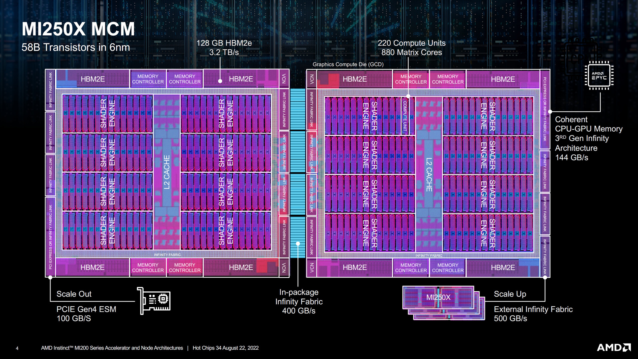
AMD in its HotChips 22 presentation released a block-diagram of its biggest AI-HPC processor, the Instinct MI250X. Based on the CDNA2 compute architecture, at the heart of the MI250X is the "Aldebaran" MCM (multi-chip module). This MCM contains two logic dies (GPU dies), and eight HBM2E stacks, four per GPU die. The two GPU dies are connected by a 400 GB/s Infinity Fabric link. They each have up to 500 GB/s of external Infinity Fabric bandwidth for inter-socket communications; and PCI-Express 4.0 x16 as the host system bus for AIC form-factors. The two GPU dies together make up 58 billion transistors, and are fabricated on the TSMC N6 (6 nm) node.
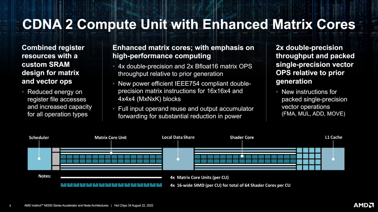
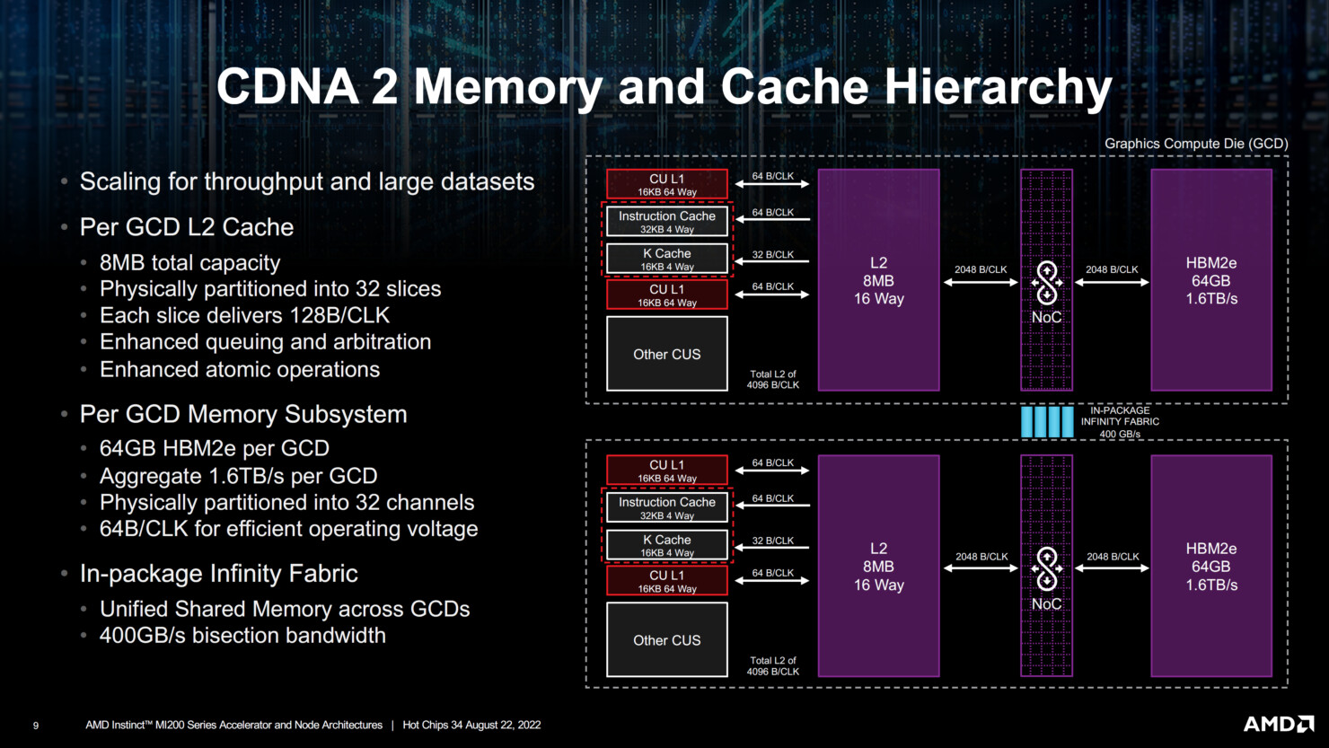
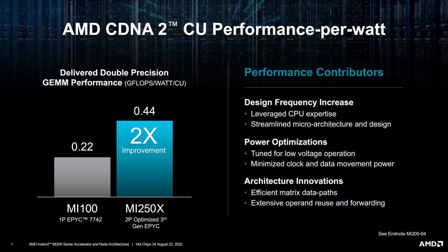
The component hierarchy of each GPU die sees eight Shader Engines share a last-level L2 cache. The eight Shader Engines total 112 Compute Units, or 14 CU per engine. The CDNA2 compute unit contains 64 stream processors making up the Shader Core, and four Matrix Core Units. These are specialized hardware for matrix/tensor math operations. There are hence 7,168 stream processors per GPU die, and 14,336 per package. AMD claims a 100% increase in double-precision compute performance over CDNA (MI100). AMD attributes this to increases in frequencies, efficient data paths, extensive operand reuse and forwarding; and power-optimization enabling those higher clocks. The MI200 is already powering the Frontier supercomputer, and is working for more design wins in the HPC space. The company also dropped a major hint that the MI300, based on CDNA3, will be an APU. It will incorporate GPU dies, core-logic, and CPU CCDs onto a single package, in what is a rival solution to NVIDIA Grace Hopper Superchip.


Source:
Wccftech
The component hierarchy of each GPU die sees eight Shader Engines share a last-level L2 cache. The eight Shader Engines total 112 Compute Units, or 14 CU per engine. The CDNA2 compute unit contains 64 stream processors making up the Shader Core, and four Matrix Core Units. These are specialized hardware for matrix/tensor math operations. There are hence 7,168 stream processors per GPU die, and 14,336 per package. AMD claims a 100% increase in double-precision compute performance over CDNA (MI100). AMD attributes this to increases in frequencies, efficient data paths, extensive operand reuse and forwarding; and power-optimization enabling those higher clocks. The MI200 is already powering the Frontier supercomputer, and is working for more design wins in the HPC space. The company also dropped a major hint that the MI300, based on CDNA3, will be an APU. It will incorporate GPU dies, core-logic, and CPU CCDs onto a single package, in what is a rival solution to NVIDIA Grace Hopper Superchip.
9 Comments on AMD Releases its CDNA2 MI250X "Aldebaran" HPC GPU Block Diagram
Nvidia: No we are!!
:nutkick::laugh:
Also, some feature could be enabled on the 400 GB that would require additional bandwidth for control. Still, they will have to improve that in the future because Apple and IBM have way better die to die interface than AMD right now.
The double (or half the HBM bandwidth per die) would have made more sense. From initial benchmark laying around the internet, they are super fast when your code can run independently on each tiles, but perf start to collapse if you need die to die access.
The tile structure should allow RDNA3 to be relatively much cheaper to manufacture than Nvidia's monolithic Lovelace. In the latest leaks, the RDNA3 GCDs for Navi 31. and 32 are really small, less than 250mm^2 if I remember correctly