News Posts matching #CoWoS-L

Return to Keyword Browsing

TSMC Could Charge Up to 20% More for CoWoS Packaging Amid AI Crunch

TSMC is reportedly considering raising prices for its CoWoS (Chip on Wafer on Substrate) advanced packaging by as much as 20%, according to supply chain sources cited by Taiwan's Commercial Times. Foundries and outsourced packaging firms are apparently weighing another round of 10% to 20% increases, as CoWoS demand has spread beyond AI GPUs to server CPUs and custom ASICs, leaving a growing backlog of unfilled orders. TSMC hasn't confirmed anything yet.

Testing is turning into a bottleneck of its own. Nomura estimates, via Seoul Economic Daily, that NVIDIA's Blackwell takes roughly four times longer than Hopper in final testing, while Rubin could need seven times as long. Packages keep growing too, with TSMC already mass producing CoWoS-L at 5.5 times the reticle limit. Tool lead times have reportedly stretched from three to six months to as long as eight months. TSMC, which usually negotiates for discounts or extra features, apparently placed this year's equipment orders at existing prices instead, which says a lot about how tight things are.

AI Chip Packaging Pushes Beyond Reticle Limits, with CoWoS-L Set to Remain the Mainstream Advanced Packaging Solution Through 2028

TrendForce's latest research into advanced semiconductor packaging reveals that GPU suppliers and hyperscale CSPs are continuing to develop increasingly powerful and versatile AI chips, making larger package sizes a key development priority for 2.5D packaging. Although TSMC's CoWoS-L faces competition from Intel's EMIB-T, its advantages in technology maturity and yield are expected to keep it the mainstream packaging solution for AI chips through 2028.

TrendForce notes that strong AI demand continues to support NVIDIA's push toward integrated GB/VR rack-scale solutions, which incorporate large numbers of chips. NVIDIA's high-end GPU shipments are expected to grow approximately 30% YoY in 2026. AMD, meanwhile, is aggressively promoting its MI400/MI450 series beginning in the second half of 2026, providing further momentum to overall shipments.

TSMC Delays Hybrid Bonding Investment for HBM, Opts for Microbumps

According to the latest report from ETNews, citing supply chain sources, TSMC is reportedly still holding back from investing in the silicon packaging technology known as hybrid bonding for HBM memory integration. For those unfamiliar, hybrid bonding creates a permanent bond between two silicon chips using embedded metal bumps that are fused together to form a single chip. Multiple dies or entire silicon wafers can be connected by stacking the back ends of two chips together. This technology eliminates traditional chip bumps and directly bonds copper interconnections between the two chips. In modern packaging, chip solder bumps, which stick out before the chip is soldered to the PCB, are roughly 100 micrometers in size, while microbumps are approximately 20 micrometers. Hybrid bonding reduces this size to 1 micrometer. Microbumps are used to interconnect silicon with other chips inside a package, as seen in CoWoS-S and CoWoS-L, where microbumps are prevalent for chip-to-interposer connections.

For TSMC, the future may involve bypassing hybrid bonding technology for packaging HBM memory and investing in microbumps that are 5 micrometers in size. Reportedly, TSMC is preparing its supply chain for 5-micrometer microbumps, which will be even smaller than what is currently available, to enhance performance in packaging. South Korean and Japanese suppliers are reportedly collaborating with TSMC to achieve this, with mass production of 5-micrometer microbumps expected in the second half of 2028. As a reminder, AMD's 3D V-Cache technology uses hybrid bonding to put SRAM on top of logic, but TSMC reportedly plans to keep integration of HBM memory into packaging on microbumps for now.

NVIDIA's "Rubin CPX" GPU Reborn with HBM4 Memory, No More GDDR7

NVIDIA has reportedly revived its "Rubin CPX" AI accelerator project, which had previously been put on hold. Today, well-known supply chain analyst Ming Chi Kuo reported that NVIDIA is reintroducing the "Rubin CPX," now featuring HBM4 memory instead of the previously planned GDDR7. Late last year, NVIDIA announced its plans to develop a specialized accelerator derived from the "Rubin" GPU family, designed for large-scale agentic AI workloads. After the announcement, the project was reportedly paused, but NVIDIA has now redesigned the memory architecture. Previously, the "Rubin CPX" was slated to have 128 GB of GDDR7 memory, but it will now include 168 GB of HBM4 memory. This GPU SKU is housed in a separate rack with configurations ranging from 64 to 256 standalone CPX GPUs per rack.

This GPU is dedicated to prefill workloads, powering racks that manage input context for LLMs and KV cache processing. Essentially, NVIDIA is separating prefill from decode tasks, with CPX GPUs handling prefill and regular "Rubin" GPUs managing decode. A rack tray with eight CPX GPUs can handle 1.34 TB of long-context prefill and the associated KV cache, all utilizing HBM4 memory for faster processing and increased bandwidth. Since the previous design did not require HBM4 integration, NVIDIA has redesigned the package, likely using TSMC's CoWoS-S or CoWoS-L for packaging.

NVIDIA Secures TSMC A16 Node for Next-Generation "Feynman" GPUs

According to supply chain sources and those close to TSMC, NVIDIA is already working on prototyping the replacement for its "Rubin" and "Rubin Ultra" GPU designs with the next-generation "Feynman" GPU microarchitecture. As noted in the latest report from DigiTimes, NVIDIA is opting for TSMC's A16 node, bypassing the N2 family of nodes entirely in favor of the more advanced 1.6 nm A16 design. Mass production is scheduled for the second half of 2028. The "Feynman" designs will rely on the backside power delivery in the A16 node, as well as on packaging technologies like 3D chiplets using SoIC, CoWoS-L 2.5D integration, and next-generation panel-level packaging.

Initially, NVIDIA will use SoIC 3D stacking technology to stack multiple chiplets into a single package, which will shorten the travel time between chips and reduce latency. These 3D chips will then be packaged side-by-side in a CoWoS-L or CoPoS packaging, creating a multi-kilowatt design capable of processing dozens of PetaFLOPS. For memory, NVIDIA will work with its partners to develop customized HBM, likely HBM4E, by the time "Feynman" reaches mass production. This customized memory includes a specialized base die that can contain logic elements like a memory controller or packet processing unit. Think of it as a way to pre-process data before it enters memory, or as a simple speedup, depending on what NVIDIA aims to achieve.

TSMC Achieves 98% Yield on CoWoS-L with 5.5x Reticle Size, 14x Comes in 2029

TSMC has reportedly achieved near-perfect packaging yields, establishing a baseline of about 98% for its current CoWoS advanced packaging. This technology accommodates a die area equivalent to 5.5 times the reticle limit, or about 858 mm². As a result, packaging 4,720 mm² worth of silicon on CoWoS-L is now possible, with only 1-2% of the packaged designs experiencing issues. This is a significant achievement for a packaging technology that went into mass production earlier this year. Although CoWoS-L has been shipping for some time, this year marks the first time a 5.5x reticle chip has been packaged on a mass production scale.

The Taiwanese manufacturing giant is also preparing for even larger designs, including up to 14x reticle size dies on a single, enormous package. This means a silicon area of 12,012 mm² will be packaged using TSMC's CoWoS, or specifically one of its variants. This technology is slated for 2029, when its A13 node is expected to be in mass production. TSMC's timelines are consistently being met with customer satisfaction, and the company continues to sell out its manufacturing and advanced packaging technologies. However, creating any design beyond the 3x reticle limit must be done carefully, as thermal warping can introduce mechanical issues. The company is constantly working with customers to overcome these challenges.

Intel's EMIB-T to Rival TSMC's CoWoS with 50% Cost Advantage, Volume Production in 2027

Intel's push for advanced packaging is reportedly attracting significant attention from external customers to Intel Foundry. However, the company's latest packaging will only begin mass production next year. Intel's Embedded Multi-die Interconnect Bridge (EMIB) enables designers to use 2D, 2.5D, and 3D building blocks to optimize cost, power, and bandwidth at the system level. EMIB is a substrate-embedded silicon bridge that provides localized, high-density die-to-die routing without the cost and area penalty of a full-size silicon interposer. For example, small silicon EMIB bridges—available in variants like EMIB-M with embedded MIM capacitors and EMIB-T with TSVs—offer low-cost, high-density shoreline connections ideal for logic-to-logic and logic-to-HBM interfaces. The EMIB-T variant, which includes TSVs, allows ASICs to gain direct access to power connections, resulting in a massive, multi-kilowatt solution on a single package.

However, this EMIB-T advanced packaging will only enter mass production next year, as Intel is currently ramping up its regular EMIB and Foveros for customers. According to Taiwan's Unimicron, which manufactures PCBs and silicon substrates, Intel's EMIB-T will reach high-volume production in 2027. The company also notes that customers, including ASIC designers like Broadcom and Meta, are considering switching from TSMC's CoWoS packaging to EMIB to reduce costs while maintaining the same benefits and even gaining more features in some areas. The price gap between EMIB-T and CoWoS (presumably CoWoS-L or CoWoS-R) can be as much as 50%, depending on whether an expensive interposer is required. This means that the costs of advanced packaging are passed back to the customer, who can then invest in other production areas.

TSMC Develops EMIB-like Technology to Compete with Intel

TSMC is reportedly developing an advanced packaging technology to rival Intel's Embedded Multi-die Interconnect Bridge (EMIB), which the company internally refers to as EMIB-like. According to sources close to The Information, TSMC's Chip-on-Wafer-on-Substrate (CoWoS) packaging might lose some customers to Intel's EMIB. As a result, TSMC has begun developing its EMIB-like technology. This development will reportedly be supported by Taiwan's Kinsus Interconnect Technology, which will assist TSMC in developing, scaling, and manufacturing the CoWoS alternative without issues. TSMC currently offers three versions of CoWoS: CoWoS-S, CoWoS-L, and CoWoS-R.

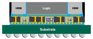
CoWoS-S is the first generation of CoWoS, utilizing a full monolithic silicon interposer with TSVs for maximum routing density and performance. Then, there is CoWoS-L that takes a hybrid approach, replacing the full silicon sheet with a more affordable organic base and embedding small localized silicon bridges (LSI) only where high-speed die-to-die communication occurs. This allows for large layouts to bypass reticle limits through bridge stitching. CoWoS-R is the third option that completely replaces silicon with an organic copper/polymer RDL interposer. It experiences a slight reduction in signal attenuation and routing density, but its mechanical flexibility makes it highly scalable and cost-effective for large-die chips.

NVIDIA's "Rubin Ultra" Reportedly Faces Issues With CoWoS-L Packaging

NVIDIA is reportedly experiencing manufacturing issues with its next-generation "Rubin Ultra" GPU design, one of the company's most ambitious chip development projects, due to the limitations of modern packaging technology. The world's largest company is already shipping customer samples of the standard "Rubin" GPUs, with mass shipments set to begin this summer. However, the current roadmap for the upgraded "Rubin Ultra" design may be encountering technological limitations, as NVIDIA's design goals are too ambitious for TSMC's packaging capabilities. Reportedly, NVIDIA plans to double the regular "Rubin" two-die package with 8 HBM4 modules into a new "Rubin Ultra" package that will include four silicon dies and 16 HBM4E modules in a single package. This configuration is scheduled for 2027, but the sheer volume of silicon may be too much for TSMC's packaging, according to Global Semi Research.

In a typical CoWoS package, TSMC usually combines multiple smaller dies and multiple HBM memory modules into a unified package that supports the entire AI build-out. However, with the ambitious "Rubin Ultra" design, NVIDIA planned to use CoWoS-L, which was expected to handle the design and concept that "Rubin Ultra" was based on. It is rumored, however, that in a 2+2 die package—meaning four dies as in this architecture—TSMC is encountering warping issues. The package—which includes a substrate—is bending in multiple directions, causing the compute dies of "Rubin Ultra" to not make complete contact with the underlying substrate. This instability means that TSMC has to explore alternatives within its packaging portfolio. One of these alternatives is a panelized approach called CoPoS, which stands for Chip-on-Panel-on-Substrate.

NVIDIA Stops China-Focused H200 "Hopper" GPU Production

NVIDIA has reportedly halted production of its China-focused H200 "Hopper" GPU at TSMC's facilities, according to multiple reports. The company has built up an inventory of 250,000 H200 GPUs, which will be available in the Chinese market for select applications that do not compromise United States national security. After NVIDIA was granted export rights to China for its H200 accelerators, the company began stockpiling these GPUs to supply AI labs across China. However, China has also restricted what its domestic companies and AI labs can import, meaning that the import of H200 GPUs is still prohibited unless a company receives a letter of exemption from Beijing. This has resulted in NVIDIA using its TSMC N5 5 nm node capacity to create about 250,000 units, which are now stored in a warehouse awaiting export approval from the U.S. administration and import approval from Chinese customs for AI labs.

Interestingly, the Financial Times and Reuters note that NVIDIA will now "reallocate" capacity from H200 production to the new "Rubin." However, these two GPU generations do not use the same manufacturing node or packaging technology. For "Hopper," NVIDIA uses TSMC's 5 nm node with CoWoS-S packaging, while "Rubin" uses a 3 nm node with CoWoS-L packaging. These reports likely refer to some conversion of manufacturing capacity involving either the node or packaging capacity that NVIDIA has secured. It is unlikely that the 5 nm semiconductor node can be converted into a 3 nm node without significant line remodeling and changes to manufacturing equipment. However, packaging can be adjusted more easily, which is likely what these reports are indicating.

TSMC's Advanced Packaging Facilities Reportedly at Max. Capacity, Insiders Whisper About Outsourcing

Over the past weekend, Taiwanese semiconductor industry moles alleged that the nation's leading foundry service is considering external advanced packaging production avenues. According to UDN Money, TSMC's "entire CoWoS series of advanced packaging products" are fully booked up—with plenty of demand coming from the usual big AI hardware players. Various flavors of Chip-on-Wafer-on-Substrate (CoWoS) exist, including the currently vaunted CoWoS-L and CoWoS-S processes. A surge in orders—reportedly coming from NVIDIA, Google, Amazon, and MediaTek—has supposedly prompted a revised strategy, beyond planned expansions of first-party facilities (primarily CoWoS-L). In order to meet lofty VIP client requests, TSMC leadership could be bolstering relationships with third-party chip packagers. The UDN Money report cites predictions made by Counterpoint, a research company—they reckon that ASE Technology (in 2026) will benefit greatly from taking on some of TSMC's "spillover."

The premier foundry business is expected to establish an improved "supply-demand" within the next year; possibly influenced by Intel's emerging capabilities—rumors have spread about Apple and Qualcomm weighing up Team Blue's advanced packaging processes. If these whispered "backup strategies" come into effect, key customers could switch loyalties by early 2028. Currently, TSMC's Arizona hub fields a massive disadvantage: a complete lack of on-site advanced packaging. Last we heard—from inside trackers—company leadership was looking into the repurposing of a planned sixth phase fabrication plant (P6 fab). This pivot could pave the way for a "fast track" deployment of US-based CoWoS activities.

TSMC Showcases Custom C-HBM4E, N3P Logic Dies Target Double Efficiency

At last week's Open Innovation Platform Ecosystem Forum in Amsterdam, TSMC provided more details over its custom HBM for the HBM4 generation, according to reports from HardwareLUXX. The company's custom C-HBM4E logic die is expected to shift to the N3P node, alongside a voltage drop from 0.8 V to 0.75 V. According to TSMC's presentation, the move targets roughly 2× better power efficiency versus today's DRAM processes. Even standard HBM4 base dies will see upgrades. Instead of using a conventional DRAM process as in HBM3E, TSMC plans to manufacture HBM4 base dies on its N12 logic node, reducing operating voltage from 1.1 V to 0.8 V. The company expects this alone to provide around a 1.5× efficiency gain. For C-HBM4E specifically, the base die doesn't just move to the N3P node, it also integrates the memory controllers directly into the stack. Those blocks normally sit on the host SoC, so the PHY becomes a fully custom design as well.

Moreover, TSMC is expanding its advanced packaging lineup with updated InFO and SoW options, but CoWoS remains the company's main growth driver. After moving from 1.5× to 3.3× reticle sizes with support for eight HBM chips, CoWoS now heads toward CoWoS-L, enabling up to 12 HBM3E/HBM4 stacks for 2026 AI parts, followed by a larger A16 generation version planned for 2027. TSMC is also securing major customers for its custom HBM logic dies. Micron has selected the foundry to build the logic base die for its HBM4E parts, with volume production planned for 2027. SK Hynix is also reportedly preparing its first custom HBM4E products for the second half of next year. According to Korea Financial Times, SK Hynix will use TSMC's 12 nm process for mainstream server-grade HBM base dies, while NVIDIA's top-end GPUs and Google's TPUs will step up to a 3 nm node.

Intel Sees 5,000 W GPUs Possible with Integrated Voltage Regulators

If the performance requirements for new AI or HPC tasks demand maximum performance density regardless of power or heat constraints, Intel has a project presentation scheduled for the ISSCC conference in February 2026. One of the topics will be a 5,000 W GPU design utilizing integrated voltage regulators (IVRs). While this may seem extreme, Intel plans to leverage advanced packaging technology, specifically the Foveros-B variant, to deliver 5 kW GPUs by 2027. As accelerators scale to support larger AI and HPC workloads, traditional board-level regulators are hitting limits in current density and transient response.

Moving voltage regulation into the package shortens current paths and reduces delivery losses. Intel Foundry and its packaging division are already exploring high-density power delivery and kW-class integrated voltage regulators. Intel's Foveros roadmap targets production-ready integrated power elements by 2027, enabling customers to evaluate IVR-enabled assemblies at scale very soon. While Foveros-B is a 2027 product, customers could potentially evaluate multi-kilowatt designs with IVRs next year. Intel is not a singled-out player with multi-kilowatt designs, as NVIDIA "Rubin" silicon is rumored to have a TDP of up to 2.3 kW for highest-end models, leading to rack-level power consumption exceeding 250 kW.

AI Boom Drives Demand for Ultra-Large Packaging as ASICs Expected to Shift from CoWoS to EMIB

TrendForce's latest investigations reveal that the rapid expansion of AI and HPC is increasing the need for heterogeneous integration, positioning advanced packaging as a strategic priority. TSMC's CoWoS platform is currently the leading solution in this area. However, as CSPs accelerate their in-house ASIC development to accommodate more complex functions, their packaging size requirements are growing substantially. As a result, some CSPs are contemplating a switch from TSMC's CoWoS to Intel's EMIB.

TrendForce notes that CoWoS connects compute logic, memory, and I/O dies via an interposer, which mounts them on a substrate. The technology has expanded to include CoWoS-S, CoWoS-R, and CoWoS-L. Demand has been strongly shifting toward CoWoS-L, which incorporates a silicon interposer into the package, as NVIDIA's Blackwell platform approaches mass production in 2025. This trend is expected to continue with NVIDIA's upcoming Rubin architecture, which will boast even larger reticle sizes.

AMD Positions Instinct MI400 Against NVIDIA Vera Rubin, MI500 Coming in 2027

At its Financial Analyst Day 2025, AMD shared new details about its upcoming Instinct MI400 and MI500 AI accelerators. The Instinct MI400 series set to launch in 2026, will be based on the new CDNA 5 architecture. AMD claims it will deliver up to 40 FP4 and 20 FP8 PFLOPs, roughly twice the compute performance of the current MI350. The GPUs also move to HBM4 memory from HMB3e, increasing capacity from 288 GB to 432 GB and raising total bandwidth from 8 TB/s to 19.6 TB/s. Each GPU provides 300 GB/s of scale-out bandwidth and adds broader AI data format support along with expanded AI pipelines. Two models are planned: the Instinct MI455X for large-scale AI training and inference, and the MI430X for HPC and sovereign AI. The MI430X features FP64 hardware based support and hybrid CPU+GPU compute capability, while retaining the same HBM4 memory subsystem as the MI455X. The MI400 series also moves away from the CoWoS-S to the CoWoS-L (Local Silicon Interconnect) advanced packaging technology.

AMD compares the MI400 lineup to NVIDIA's upcoming Vera Rubin series, claiming similar compute performance and memory bandwidth, but 1.5× higher memory capacity and scale-out bandwidth. During her presentation, Dr. Lisa Su said that AMD's Instinct MI400 accelerators will be available to clients and partners from day one, while the next-generation MI500 is already in advanced design stages. AMD is also now moving to an annual refresh cycle for its Instinct products, confirming that its next-gen MI500 series will be launched in 2027.

NVIDIA to Tap TSMC's A16 Node for "Feynman" GPUs

NVIDIA is preparing a significant change in its chip strategy for its next-generation GPU design, codenamed "Feynman", as the first customer of TSMC's A16 process. This choice breaks NVIDIA's long-running pattern of adopting slightly older nodes to extract greater efficiency and performance gains for its datacenter accelerators. NVIDIA's biggest AI dies are enormous, at 104 billion transistors currently per each "Blackwell Ultra" die and occupying areas that are breaking reticle limits. Such a scale typically favors one or two generations old nodes to protect yield and thermal characteristics. To keep up with the compute demand, NVIDIA appears to be adapting its architectures to A16 while keeping other families like "Rubin" on refined N3P variants and paired with CoWoS-L packaging.

The most appealing aspect of the A16 node will be its backside power delivery, which separates power and signal routing to reduce losses and simplify floor planning. Implementations range from buried power rails that still use a front-side lowest metal layer to power vias that reach the rear side. TSMC's Super Power Rail concept enables power to be delivered directly to the transistor's source and drain terminals, resulting in lower resistance. Those choices affect efficiency, layout, and thermal behavior. Power demands for high-end AI accelerators are rising fast. Current flagship solutions already draw about 1,400 W in Blackwell Ultra, and next-generation Rubin designs are expected to exceed 2,300 W. Hence, node selection will be critical for the next-generation Feynman design, given its multi-gigawatt power requirement. If A16 reaches volume production on schedule, first silicon could arrive in late 2027 or early 2028.

NVIDIA "Rubin" Platform Enters Trial Production at TSMC, CEO Jensen Huang Confirms

NVIDIA confirmed today that it has taped out six distinct "Rubin" chips, which signals something more than a typical product refresh. Company CEO Jensen Huang, speaking during a visit to Taiwan, said NVIDIA already handed multiple Rubin designs to TSMC and that those dies are now entering fab qualification ahead of trial production. Rubin is intended to be a platform-level upgrade, rather than a simple GPU update, with changes extending across processors, networking gear, and interconnect silicon. Customers and cloud operators will be watching closely as NVIDIA prepares what it describes as the next major compute platform. According to Jensen, the taped designs include a dedicated CPU, new GPU variants, a scale-up NVLink switch, and a silicon photonics processor aimed at improving rack-scale connectivity and off-chip optics.

Rubin will adopt chiplet partitioning for the first time in NVIDIA's product line and is planned for TSMC's N3P process with CoWoS-L packaging. Memory is expected to transition to next-generation HBM4 stacks to sustain higher bandwidth, featuring a custom base die. The physical compute die layout will utilize a larger reticle area compared to the current generation. NVIDIA says it is coordinating hardware changes with software updates, including compiler and runtime improvements that will leverage the new topology. The company projects market introductions around 2026 for Rubin and 2027 for Rubin Ultra, depending on trial production and yields. Early validation is already underway, covering thermal, power, and interconnect scenarios. The Rubin transition from Blackwell is shaping up to be a big step, and in the new generation of AI token factories, we need more powerful chips with million-scale data centers.

TSMC Prepares "CoPoS": Next-Gen 310 × 310 mm Packages

As demand for ever-growing AI compute power continues to rise and manufacturing advanced nodes becomes more difficult, packaging is undergoing its golden era of development. Today's advanced accelerators often rely on TSMC's CoWoS modules, which are built on wafer cuts measuring no more than 120 × 150 mm in size. In response to the need for more space, TSMC has unveiled plans for CoPoS, or "Chips on Panel on Substrate," which could expand substrate dimensions to 310 × 310 mm and beyond. By shifting from round wafers to rectangular panels, CoPoS offers more than five times the usable area. This extra surface makes it possible to integrate additional high-bandwidth memory stacks, multiple I/O chiplets and compute dies in a single package. It also brings panel-level packaging (PLP) to the fore. Unlike wafer-level packaging (WLP), PLP assembles components on large, rectangular panels, delivering higher throughput and lower cost per unit. Systems with PLP will be actually viable for production runs and allow faster iterations over WLP.

TSMC will establish a CoPoS pilot line in 2026 at its Visionchip subsidiary. In 2027, the pilot facility will focus on refining the process, to meet partner requirements by the end of the year. Mass production is projected to begin between the end of 2028 and early 2029 at TSMC's Chiayi AP7 campus. That site, chosen for its modern infrastructure and ample space, is also slated to host production of multi-chip modules and System-on-Wafer technologies. NVIDIA is expected to be the launch partner for CoPoS. The company plans to leverage the larger panel area to accommodate up to 12 HBM4 chips alongside several GPU chiplets, offering significant performance gains for AI workloads. At the same time, AMD and Broadcom will continue using TSMC's CoWoS-L and CoWoS-R variants for their high-end products. Beyond simply increasing size, CoPoS and PLP may work in tandem with other emerging advances, such as glass substrates and silicon photonics. If development proceeds as planned, the first CoPoS-enabled devices could reach the market by late 2029.

NVIDIA Reportedly Progressing Well with "Rubin" AI GPU Development - Insiders Foresee Q3'25 Sampling

Over a year ago, industry moles started chattering about a potential "late 2025" launch of NVIDIA "Rubin" AI accelerators/ GPUs. According to older rumors, one of the successors to current-gen "Blackwell" hardware could debut in chiplet-based "R100" form. Weeks ahead of Christmas 2024, Taiwanese insider reports pointed to Team Green's development of the "Rubin" AI project being sixth months ahead of schedule. Despite this extra positive outlook, experts surmised that the North American giant would not be rushing out shiny new options—especially with the recent arrival of "Blackwell Ultra" products. A lot of leaks seem to be coming from sources at (or adjacent to) TSMC.

Taiwan's top foundry service is reportedly in the "Rubin" equation; with a 3 nm (N3P) node process and CoWoS-L packaging linked to "R100." According to local murmurs, the final "taping out"—of Rubin GPUs and Vera CPUs—is due for completion this month. Trial production is expected run throughout the summer, with initial samples being ready for distribution by September. According to a fresh Ctee TW news report, unnamed supply chain participants reckon that NVIDIA's "new chip development schedule is smoother than before, and mass production (of Rubin and Vera chips) will begin as early as 2026." In theory, the first publicly exhibited final examples could turn up at CES 2026.

TSMC Outlines Roadmap for Wafer-Scale Packaging and Bigger AI Packages

At this year's Technology Symposium, TSMC unveiled an engaging multi-year roadmap for its packaging technologies. TSMC's strategy splits into two main categories: Advanced Packaging and System-on-Wafer. Back in 2016, CoWoS-S debuted with four HBM stacks paired to N16 compute dies on a 1.5× reticle-limited interposer, which was an impressive feat at the time. Fast forward to 2025, and CoWoS-S now routinely supports eight HBM chips alongside N5 and N4 compute tiles within a 3.3× reticle budget. Its successor, CoWoS-R, increases interconnect bandwidth and brings N3-node compatibility without changing that reticle constraint. Looking toward 2027, TSMC will launch CoWoS-L. First up are large N3-node chiplets, followed by N2-node tiles, multiple I/O dies, and up to a dozen HBM3E or HBM4 stacks—all housed within a 5.5× reticle ceiling. It's hard to believe that eight HBM stacks once sounded ambitious—now they're just the starting point for next-gen AI accelerators inspired by AMD's Instinct MI450X and NVIDIA's Vera Rubin.

Integrated Fan-Out, or InFO, adds another dimension with flexible 3D assemblies. The original InFO bridge is already powering AMD's Instinct cards. Later this year, InFO-POP (package-on-package) and InFO-2.5D arrive, promising even denser chip stacking and unlocking new scaling potential on a single package, away from the 2D and 2.5D packaging we were used to, going into the third dimension. On the wafer scale, TSMC's System-on-Wafer lineup—SoW-P and SoW-X—has grown from specialized AI engines into a comprehensive roadmap mirroring logic-node progress. This year marks the first SoIC stacks from N3 to N4, with each tile up to 830 mm² and no hard limit on top-die size. That trajectory points to massive, ultra-dense packages, which is exactly what HPC and AI data centers will demand in the coming years.

Cadence and TSMC Advance AI and 3D-IC Chip Design with Certified Design Solutions for TSMC A16 and N2P Process

Cadence today announced it is furthering its longstanding collaboration with TSMC to accelerate time to silicon for 3D-IC and advanced-node technologies through certified design flows, silicon-proven IP and ongoing technology collaboration. As a leading provider of IP for TSMC N2P, N5 and N3 process nodes, Cadence continues to deliver cutting-edge AI-driven design solutions to the TSMC ecosystem for multiple horizontal applications from chiplets and SoCs to advanced packaging and 3D-ICs. The deep collaboration encompasses certified tools and flows for TSMC's N2P and A16 technologies, paves the way for TSMC's A14 and further unlocks 3D-IC possibilities by extending support for TSMC 3DFabric design and packaging. In addition, Cadence and TSMC are extending tool certification for newly announced TSMC N3C technology based on available N3P design solutions.

Cadence is driving innovation in AI chip design with certified tools and optimized IP for TSMC's advanced N2P and A16 process technologies. Reinforcing its memory IP leadership, Cadence offers TSMC9000 pre-silicon-certified DDR5 12.8G IP for N2P. Cadence digital, custom/analog design and thermal analysis solutions are certified for TSMC N2P and A16 technologies. Combined with continued collaboration on AI-driven digital design solutions for N2P, including leveraging large language models (LLMs), these advancements play an important role in improving digital design flows for future process nodes.

TSMC Reserves 70% of 2025 CoWoS-L Capacity for NVIDIA

Rumors previously suggested that NVIDIA might scale back its CoWoS orders from TSMC. However, according to a report from Economic Daily News, orders for TSMC's advanced packaging have instead seen a surge. NVIDIA's Blackwell architecture GPUs are in strong demand, leading the company to secure over 70% of TSMC's CoWoS-L advanced packaging capacity for 2025. Shipment volumes are projected to rise by more than 20% each quarter, with total annual shipments expected to surpass 2 million units.

Meanwhile, following the U.S. announcement of the Stargate project—which is anticipated to drive new AI server demand—NVIDIA is reportedly considering placing additional orders with TSMC. During TSMC's earnings call in January, Chairman C.C. Wei stated that the company is continuously expanding its advanced packaging capacity to keep pace with customer demand. According to reports, advanced packaging revenue accounted for roughly 8% in 2024 and is projected to exceed 10% in 2025.

NVIDIA "Blackwell" NVL72 Servers Reportedly Require Redesign Amid Overheating Problems

According to The Information, NVIDIA's latest "Blackwell" processors are reportedly encountering significant thermal management issues in high-density server configurations, potentially affecting deployment timelines for major tech companies. The challenges emerge specifically in NVL72 GB200 racks housing 72 GB200 processors, which can consume up to 120 kilowatts of power per rack, weighting a "mere" 3,000 pounds (or about 1.5 tons). These thermal concerns have prompted NVIDIA to revisit and modify its server rack designs multiple times to prevent performance degradation and potential hardware damage. Hyperscalers like Google, Meta, and Microsoft, who rely heavily on NVIDIA GPUs for training their advanced language models, have allegedly expressed concerns about possible delays in their data center deployment schedules.

The thermal management issues follow earlier setbacks related to a design flaw in the Blackwell production process. The problem stemmed from the complex CoWoS-L packaging technology, which connects dual chiplets using RDL interposer and LSI bridges. Thermal expansion mismatches between various components led to warping issues, requiring modifications to the GPU's metal layers and bump structures. A company spokesperson characterized these modifications as part of the standard development process, noting that a new photomask resolved this issue. The Information states that mass production of the revised Blackwell GPUs began in late October, with shipments expected to commence in late January. However, these timelines are unconfirmed by NVIDIA, and some server makers like Dell confirmed that these GB200 NVL72 liquid-cooled systems are shipping now, not in January, with CoreWave GPU cloud provider as a customer. The original report could be using older information, as Dell is one of NVIDIA's most significant partners and among the first in the supply chain to gain access to new GPU batches.

NVIDIA Resolves "Blackwell" Yield Issues with New Photomask

During its Q2 2024 earnings call, NVIDIA confirmed that its upcoming Blackwell-based products are facing low-yield challenges. However, the company announced that it has implemented design changes to improve the production yields of its B100 and B200 processors. Despite these setbacks, NVIDIA remains optimistic about its production timeline. The tech giant plans to commence the production ramp of Blackwell GPUs in Q4 2024, with expected shipments worth several billion dollars by the end of the year. In an official statement, NVIDIA explained, "We executed a change to the Blackwell GPU mask to improve production yield." The company also reaffirmed that it had successfully sampled Blackwell GPUs with customers in the second quarter.

However, NVIDIA acknowledged that meeting demand required producing "low-yielding Blackwell material," which impacted its gross margins. During an earnings call, NVIDIA's CEO Jensen Huang assured investors that the supply of B100 and B200 GPUs will be there. He expressed confidence in the company's ability to mass-produce these chips starting in the fourth quarter. The Blackwell B100 and B200 GPUs use TSMC's CoWoS-L packaging technology and a complex design, which prompted rumors about the company facing yield issues with its designs. Reports suggest that initial challenges arose from mismatched thermal expansion coefficients among various components, leading to warping and system failures. However, now the company claims that the fix that solved these problems was a new GPU photomask, which bumped yields back to normal levels.

NVIDIA's New B200A Targets OEM Customers; High-End GPU Shipments Expected to Grow 55% in 2025

Despite recent rumors speculating on NVIDIA's supposed cancellation of the B100 in favor of the B200A, TrendForce reports that NVIDIA is still on track to launch both the B100 and B200 in the 2H24 as it aims to target CSP customers. Additionally, a scaled-down B200A is planned for other enterprise clients, focusing on edge AI applications.

TrendForce reports that NVIDIA will prioritize the B100 and B200 for CSP customers with higher demand due to the tight production capacity of CoWoS-L. Shipments are expected to commence after 3Q24. In light of yield and mass production challenges with CoWoS-L, NVIDIA is also planning the B200A for other enterprise clients, utilizing CoWoS-S packaging technology.
Return to Keyword Browsing
Nov 19th, 2026 11:58 CST change timezone

New Forum Posts

Popular Reviews

TPU on YouTube

Controversial News Posts