Friday, December 5th 2025

TSMC Arizona Supposedly Considering Conversion of "Phase 6 Fab" into Advanced Packaging Facility
Pleasing progress at TSMC's Arizona location has resulted in company leadership expediting a "push into advanced node deployment." Mid-October reports cited an increased domestic demand for 2 nm-class wafer products. Despite the foundry industry leader and NVIDIA's public celebration of debut "made in the USA" NVIDIA "Blackwell" wafers, TSMC's Phoenix-adjacent campus lacks in one key area: advanced packaging. Not long after the conclusion of festivities, computer hardware news outlets highlighted Fab 21-produced (4 nm) Blackwell products being sent overseas—specifically, back to Taiwan—for Chip on Wafer on Substrate (CoWoS) treatments.
Later on in October, TechPowerUp's AleksandarK covered the importance of advanced packaging on North American soil. His special editorial piece focuses on Intel Foundry's potential advantages in this area of expertise; thus poised to take a leading position within the region's semiconductor industry. Yesterday, Taiwan's Liberty Times outlined a major near-future change for one section's of TSMC Arizona's vast spread: "(leadership) plans to convert the land of the planned sixth phase fabrication plant (P6 fab) into an advanced packaging (AP) plant. If the construction goes smoothly, it is expected to be installed as early as the end of 2027 and enter the pre-production stage." Some of the claimed inside track timelines seems to roughly align with previous reports of TSMC and Amkor Technology's $7 billion forthcoming "advanced outsourced semiconductor packaging and testing" facility.

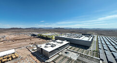
Sources:
Liberty Times Taiwan, TrendForce, Wccftech, Semi Vision (Arizona site layout)
Later on in October, TechPowerUp's AleksandarK covered the importance of advanced packaging on North American soil. His special editorial piece focuses on Intel Foundry's potential advantages in this area of expertise; thus poised to take a leading position within the region's semiconductor industry. Yesterday, Taiwan's Liberty Times outlined a major near-future change for one section's of TSMC Arizona's vast spread: "(leadership) plans to convert the land of the planned sixth phase fabrication plant (P6 fab) into an advanced packaging (AP) plant. If the construction goes smoothly, it is expected to be installed as early as the end of 2027 and enter the pre-production stage." Some of the claimed inside track timelines seems to roughly align with previous reports of TSMC and Amkor Technology's $7 billion forthcoming "advanced outsourced semiconductor packaging and testing" facility.


10 Comments on TSMC Arizona Supposedly Considering Conversion of "Phase 6 Fab" into Advanced Packaging Facility
Smells like someone is seeing a drop in demand for the future.
With the growth of Chiplet based products the need for CoWoS is going to grow in the short term.
en.wikipedia.org/wiki/TSMC_Arizona
Plent of extra capacity going on there and probably just bringing up the packaging/finishing aspect up a little earlier than planned.
That's a topic for a good article...
@T0@st
@AleksandarK