News Posts matching #Flash Memory

Return to Keyword Browsing

Kioxia to Expand 3D Flash Memory Production Capacity with the New Fab3 at Kitakami Plant

Kioxia Corporation, a world leader in memory solutions, announced today that it has commenced site preparation and other related work for the construction of Fab3, a new state-of-the-art manufacturing facility at the Kitakami Plant in Iwate Prefecture, Japan, to expand production capacity for advanced three-dimensional flash memory BiCS FLASH. Fab3 will be constructed on land south of Fab2, targeting operations to commence in fiscal 2029.

The flash memory market is expected to continue to expand significantly in the medium to long term, driven by agentic AI, physical AI, and on-device AI. Through the construction of Fab3, Kioxia aims to meet rising market demand by expanding production and ensuring stable supply of cutting-edge flash memory products.

Kioxia and Sandisk Unveil New High-Performance QLC 3D Flash Memory

Kioxia Corporation, a subsidiary of Kioxia Holdings Corporation (TOKYO: 285A) and Sandisk Corporation (Nasdaq: SNDK) today unveiled their new 9th-generation, high-performance 2 Tb QLC 3D flash memory technology designed to support the growing storage demands of AI-driven infrastructure. The technology demonstrates how architectural innovation can help storage advance at the fast pace required by AI-driven workloads, while supporting more capital-efficient manufacturing.

Leveraging the companies' CMOS directly Bonded to Array (CBA) architecture, the new technology combines an advanced CMOS wafer with a proven memory-array platform, along with significant design and device innovation, to deliver performance improvements and enable faster deployment of advanced storage solutions for cloud and data-intensive applications. Compared with the previous 8th-generation 2 Tb QLC, the new technology delivers higher write and read bandwidth due to a 6-plane architecture and performance enhancements, and better write and read power efficiency. And it also delivers a NAND interface speed of 4.8 Gb/s, a 33% improvement over 8th-generation devices.

Memblaze Showcases PBlaze7 Series Enterprise SSDs at FMS 2026

On August 4, FMS 2026 (The Future of Memory and Storage), a premier global event in the memory and storage technology industry, officially opened in Santa Clara, California. Beijing Memblaze Technology Co., Ltd. (Memblaze), a world-renowned provider of enterprise PCIe SSDs, showcased its PBlaze7 series products. Highlighting core advantages in high performance, ultra-low latency, high reliability, and high density, Memblaze is building a robust storage foundation focused on the evolution of AI infrastructure, while exploring new enterprise storage opportunities with global customers and partners.

FMS 2026 brought together leading global memory and storage vendors, key ecosystem players, and industry clients to showcase cutting-edge technical achievements and product innovations. Driven by new demands from evolving AI technologies, intense discussions took place around groundbreaking high-bandwidth, low-latency storage and interconnect technologies—such as HBM4/HBM4e, higher-layer 3D NAND stacking, PCIe 6.0, and optical interconnects. Other key topics included data management for AI workloads, KV Cache optimization, performance tuning for ultra-large capacity SSDs, and storage software stack optimizations, jointly painting a new blueprint for AI-era storage architecture.

Samsung Unveils Next-Gen 3D-Memory Vision at FMS 2026

Samsung Electronics a global leader in advanced memory technology, today showcased its latest AI memory innovations at Future of Memory and Storage (FMS) 2026 in Santa Clara, California.

With broad expertise spanning DRAM, NAND, enterprise storage and relevant advanced semiconductor technologies, Samsung presented its latest AI memory portfolio and technology roadmap, including a preview of its zHBM and zNAND-O concept models, the industry-first introduction of its V10 BV-NAND with 400-plus layers and a comprehensive range of solutions designed to advance future AI infrastructure. Samsung is also featuring its AI cloud server-inspired booth at FMS 2026, where approximately 30 memory and storage technologies are on display.

Kioxia and Sandisk Unveil 10th-Gen 332-Layer QLC NAND with 4.8 Gb/s Interface Speeds

Kioxia Corporation, a subsidiary of Kioxia Holdings Corporation (TOKYO: 285A) and Sandisk Corporation (Nasdaq: SNDK) today unveiled their next-generation Quad-Level-Cell (QLC) 3D flash memory technology, which delivers up to 60% increase in bit density compared to their 8th-generation, surpassing 37 Gb/mm² and setting the industry benchmark for bit density, performance and power efficiency.

Leveraging the companies' revolutionary CMOS directly Bonded to Array (CBA) technology which fabricates CMOS logic and the memory array on separate wafers before bonding them together with high-precision wafer-to-wafer alignment, the new generation improves read and write bandwidth compared to the 8th-generation 3D flash memory and becomes the industry's first QLC 3D flash memory technology to reach a 4.8 Gb/s interface.

Kioxia Announces UFS 5.0 Embedded Flash Memory Devices

Kioxia Corporation, a world leader in memory solutions, today announced its UFS 5.0 embedded flash memory solutions, designed to deliver the performance, efficiency and capacity required for the next generation of AI-enabled mobile and edge devices. The new solutions will be demonstrated next week at FMS: the Future of Memory and Storage and are now available as commercial samples in 1 TB and 512 GB capacities. Mass production is expected to begin by the end of 2026.

Built on the latest JEDEC UFS 5.0 standard, Kioxia's new devices leverage the MIPI M-PHY v6.0 physical layer and UniPro v3.0 protocol, including HS-Gear6 operation, to support theoretical interface speeds of up to 46.6 Gb/s per lane and approximately 10.8 GB/s of effective dual-lane read/write performance. As AI workloads continue moving onto devices, storage performance is becoming increasingly important. Large language models, multimodal AI, advanced imaging and real-time inference require significantly faster movement of data between storage and compute. Until now, UFS read performance has been a limiting factor for increasingly sophisticated on-device AI, constraining how quickly large language models and other AI workloads can access data. Kioxia's UFS 5.0 helps remove these bottlenecks, enabling faster application loading, greater responsiveness and unprecedented user experience across on-device AI applications when compared to UFS 4.1.

Sandisk Announces Sampling of BiCS10 1 Tb TLC 3D NAND Flash Memory

Sandisk Corporation (Nasdaq: SNDK) today announced it is sampling its BiCS10 1 Tb TLC, its 10th-generation 3D NAND flash memory technology. BiCS10 applies advanced lateral scaling techniques to achieve industry-leading 1 Tb TLC memory density greater than 29 Gb/mm², improving bit density by 59 percent while delivering up to 4.8 Gb/s interface speed, a 33 percent improvement compared with 8th generation 3D flash memory currently in mass production.

Built on Sandisk's proven Bit-Cost Scalable (BiCS) 3D NAND architecture and CMOS directly Bonded to Array (CBA) technology, BiCS10 TLC also enhances data input/output power efficiency, reducing power consumption by 10 percent for input and 34 percent for output compared to the previous BiCS8 generation.

Kioxia Commences Sample Shipments of 10th-Generation BiCS FLASH Devices

Kioxia Corporation, a world leader in memory solutions, today announced that it has commenced sample shipments of 1 Tb (terabit) Triple-Level-Cell (TLC) memory devices utilizing its 10th-generation BiCS FLASH 3D flash memory technology. These will be primarily integrated into the company's enterprise and data center SSDs, strengthening Kioxia's lineup to meet the growing demand for AI storage, which requires higher performance, higher capacity, and lower power consumption. These new products will be manufactured using state-of-the-art equipment at Kioxia's Kitakami Plant Fab2 facility in Iwate Prefecture, Japan.

By leveraging innovative CMOS directly Bonded to Array (CBA) technology and On-Pitch Select Gate Drain (OPS) technology, both adopted since the 8th-generation BiCS FLASH, the 10th-generation technology achieves a NAND interface speed of 4.8 Gb/s, a 33% improvement over the 8th generation. Bit density has increased by 59% by stacking 332 layers and improving lateral density. Additionally, write and read power efficiencies have improved by 18% and 30% respectively, helping to reduce power consumption in data centers and enterprise infrastructure.

Combined Revenue of Top Five Global NAND Flash Suppliers Rose by 83.7% QoQ for 1Q26 as Supply Shortages Drove Price Hikes

According to TrendForce's latest survey of the NAND Flash industry, CSPs worldwide experienced an exponential surge in demand for enterprise SSDs in 1Q26 due to the need for high-speed data transmission and the massive data storage capacities required to build out AI server infrastructure. Additionally, a persistent structural shortage of traditional HDDs has led a significant volume of storage-related orders to shift toward QLC enterprise SSDs. Amidst this soaring demand and constrained supply, NAND Flash suppliers' ASPs broadly exceeded expectations. Hence, the combined revenue of the world's top five NAND Flash suppliers jumped 83.7% QoQ, surpassing US$38.9 billion.

Moving into 2Q26, the supply-demand imbalance is expected to persist. Although rising memory costs and higher end-product prices have dampened smartphone and PC demand, brisk server orders will fill this gap. NAND Flash suppliers generally anticipate continued growth in their shipments through the second quarter, and their pricing strategies are expected to sustain elevated ASPs.

Phison Rescales Local AI Inferencing with Flash Memory Expansion

Phison Electronics (8299TT), a global leader in NAND flash controllers and storage solutions, today announced its GTC showcase at booth 119, demonstrating how multi-tier memory architecture supports larger models and long-context inference on NVIDIA-powered local AI platforms. The industry is facing a growing memory constraint while demand for AI-ready platforms continues to surge. Fine-tuning and inference on proprietary data require massive compute and memory resources, creating investment challenges for organizations. These rising solution costs and workflow bottlenecks are slowing time-to-market for revenue-generating innovation. To address this challenge, Phison introduced aiDAPTIV technology for local and edge AI use cases. By leveraging Pascari SSDs as a new AI memory tier, aiDAPTIV technology intelligently extends and manages AI working memory across GPU memory, system RAM and flash.

Today's announcement showcases how aiDAPTIV applies these multi-tier memory architecture principles to local AI systems as NVIDIA AI infrastructure advances GPU memory capabilities to support inference workloads in data center environments. Built on high-endurance flash optimized for sustained paging and context retention, aiDAPTIV supports memory-intensive inference and fine-tuning workloads under fixed hardware configurations. The aiDAPTIV flash-based memory tier enables organizations to support these evolving workloads on local systems while maintaining data privacy and improving long-term infrastructure efficiency.

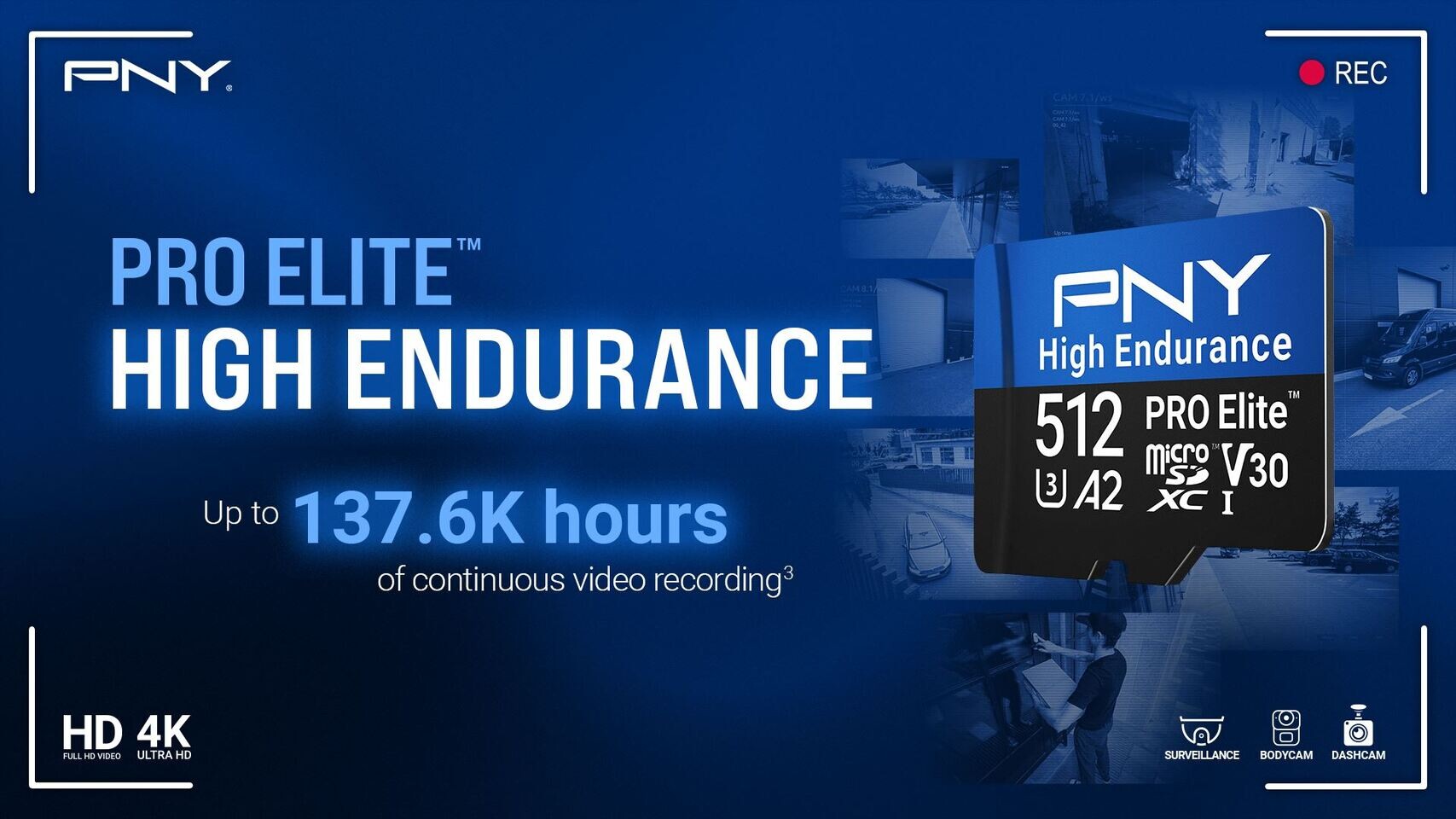
Kioxia Sampling UFS 5.0 Embedded Flash Memory Devices

Kioxia Corporation, a world leader in memory solutions, today announced that it has begun shipping evaluation samples of embedded flash memory compatible with the next-generation UFS standard, UFS 5.0, which is currently being standardized by JEDEC.

UFS 5.0 is a new standard for embedded flash storage currently being developed by JEDEC to meet the performance requirements of next-generation mobile devices such as high-end smartphones equipped with on-device AI functions. It utilizes MIPI M-PHY version 6.0 for the physical layer and UniPro version 3.0 for the protocol. M-PHY version 6.0 introduces the new HS-GEAR6 mode, theoretically supporting an interface speed of up to 46.6 Gbps per lane; with 2 lanes, UFS 5.0 can achieve approximately 10.8 GB/s of effective read/write performance.

KIOXIA Introduces QLC UFS 4.1 Embedded Flash Memory Devices for High-Capacity Mobile Storage

KIOXIA America, Inc. today announced that it has begun sampling new Universal Flash Storage (UFS) Ver. 4.1 embedded memory devices with 4-bit-per-cell, quadruple-level cell (QLC) technology. Designed for read-intensive applications and high-capacity storage needs, the new devices are powered by KIOXIA's 8th generation BiCS FLASH 3D flash memory technology.

QLC UFS offers a higher bit density than traditional TLC UFS, making it suitable for mobile applications that require higher storage capacities. Advancements in controller technology and error correction have enabled QLC technology to achieve this while maintaining competitive performance.

Flash Memory and Chip Prices Rise as TSMC, SanDisk Announce Hikes

TSMC will implement significant price adjustments beginning in 2026, targeting advanced nodes below 5 nm with increases ranging from 5% to 10%, TrendForce reports. The world's largest contract chipmaker currently sells 3 nm wafers for approximately $20,000 each, but expects 2 nm wafers to exceed $30,000 when mass production begins in late 2025. These changes affect major customers including Apple and NVIDIA. TSMC's investments of over $65 billion in Arizona facilities represent a key factor in this pricing strategy since the U.S. plant started 4 nm production in early 2025. AMD's Lisa Su confirmed these overseas facilities cost 5-20% more to operate than Taiwan-based manufacturing due to various operational factors. The price increases show TSMC's efforts to maintain gross margins above 53% while Arizona operations are expected to reduce company-wide margins by 2-3% initially, potentially reaching 3-4% over time.

Meanwhile SanDisk announced a 10% price increase for all channel partners and consumer products, effective for new orders placed after September 5th. SanDisk says this decision is based on the increasing demand from AI applications, data centers, and mobile devices. The company plans regular price reviews with potential future modifications, while TSMC may reduce prices for mature manufacturing processes where cost pressures remain manageable.

Kioxia Achieves Successful Prototyping of 5 TB Large-Capacity and 64 GB/s High-Bandwidth Flash Memory Module

Kioxia Corporation, a world leader in memory solutions, has successfully developed a prototype of a large-capacity, high-bandwidth flash memory module essential for large-scale artificial intelligence (AI) models. This achievement was made within the "Post-5G Information and Communication Systems Infrastructure Enhancement R&D Project (JPNP20017)" commissioned by the New Energy and Industrial Technology Development Organization (NEDO), Japan's national research and development agency. This memory module features a large capacity of five terabytes (TB) and a high bandwidth of 64 gigabytes per second (GB/s).

To address the trade-off between capacity and bandwidth that has been a challenge with DRAM-based conventional memory modules, Kioxia has developed a new module configuration utilizing daisy-chained connections with beads of flash memories. We have also developed high-speed transceiver technology enabling bandwidths of 128 gigabits per second (Gbps), along with techniques to enhance flash memory performance. These innovations have been effectively applied to both memory controllers and memory modules.

SSSTC Launches World's First Industrial M.2 SSD Featuring KIOXIA's 8th generation BiCS FLASH Technology

Solid State Storage Technology Corporation (SSSTC) proudly announces the launch of the SSSTC CA8 Series, the world's first industrial M.2 SSD built with BiCS FLASH generation 8 3D flash memory technology and a PCIe Gen 5 x4 interface. Offered in the industry-standard M.2 2280 form factor, the SSSTC CA8 Series is available in 512 GB, 1 TB, 2 TB, and 4 TB capacities.

The SSSTC CA8 Series complies with PCIe 5.0 and NVMe 2.0, supporting ultra-high-speed data access with transfer rates up to 32 GT/s per-lane—doubling the throughput of PCIe 4.0 interface. With SLC caching, the SSSTC CA8 Series achieves sequential read speeds of up to 14,000 MB/s and write speeds up to 12,000 MB/s, along with random performance of up to 2,000K IOPS (read) and 1,600K IOPS (write)—making it one of the fastest industrial SSDs on the market.

FMS 2025: SK hynix Presents Future of AI and Storage Through Innovative Tech Showcase

SK hynix presented its cutting-edge DRAM, NAND, and AI memory solutions at FMS: the Future of Memory and Storage 2025 in Santa Clara, California from August 5-7, reinforcing its global memory leadership.

Now in its 19th year, FMS, previously known as the Flash Memory Summit, rebranded in 2024. It adopted the name the Future of Memory and Storage to reflect the transformative influence of the AI era. The event's scope was also expanded from focusing solely on flash memory to covering the full spectrum of memory and storage technologies, including DRAM.

Sandisk to Collaborate with SK hynix to Drive Standardization of High-Bandwidth Flash Memory Technology

Sandisk Corporation (NASDAQ: SNDK) today announced it has signed a landmark Memorandum of Understanding (MOU) with SK hynix to work together to establish the specification for High Bandwidth Flash - a new technology designed to deliver breakthrough memory capacity and performance for the next generation of AI inferences. Through this collaboration, the companies expect to standardize the specification, define technology requirements and explore the creation of a technology ecosystem for High Bandwidth Flash.

"By collaborating with SK hynix to define the High Bandwidth Flash specification, we are addressing the critical need for scalable memory in the AI industry," said Alper Ilkbahar, Executive Vice President and Chief Technology Officer, and HBF Technical Advisory Board member at Sandisk. "This collaboration accelerates innovation and will offer the industry new tools to handle the exponential data demands of tomorrow's applications. Our work will help provide an effective solution to meet the world's technology needs and exceeds expectations of our respective customers."

KIOXIA Showcases Breakthrough Flash Storage Solutions at FMS 2025

Kioxia group, a world leader in memory solutions, will once again take center stage at FMS: the Future of Memory and StorageA new window will open. to spotlight how its flash memory and SSD innovations are driving scalable, efficient infrastructure for artificial intelligence (AI). With a focus on real-world applications and performance gains, Kioxia will demonstrate how its latest solutions meet the evolving demands of AI across data center and enterprise environments.

Kioxia will spotlight its newest products, including the high-capacity KIOXIA LC9 Series - the industry's first 245.76 terabyte (TB) NVMe SSD. Additional highlights include the KIOXIA CM9 Series and KIOXIA CD9P Series SSDs built with the company's BiCS FLASH generation 8 3D flash memory, delivering performance, power efficiency, and versatility. Kioxia will also display 1 terabit (Tb) 3bit/cell (TLC) products with BiCS FLASH generation 9 and generation 10 3D flash memory technology. BiCS FLASH generation 9 and generation 10 3D flash memory incorporate interface standards, Toggle DD6.0, and leverage the SCA (Separate Command Address) protocol and a novel command address input method of its interface, and PI-LTT (Power Isolated Low-Tapped Termination) technology, which provide improvements in data input and output speed and power consumption reduction.

KIOXIA Launches UFS Ver. 4.1 Embedded Flash Memory Devices for Automotive Applications

KIOXIA America, Inc. today announced that it has begun sampling new Universal Flash Storage (UFS) Ver. 4.1 embedded memory devices designed for automotive applications. Engineered to meet the rigorous demands of next-generation in-vehicle systems, these new devices deliver significant performance, flexibility, and diagnostic enhancements - powered by KIOXIA's 8th generation BiCS FLASH 3D flash memory technology and in-house designed controller technology.

Available in capacities of 128 gigabytes (GB), 256 GB, 512 GB and 1 terabyte (TB), the new UFS 4.1 devices are designed to fit the needs of infotainment, ADAS, telematics, domain controllers, and vehicle computers. They meet AEC-Q100/1044 Grade 2 standards, supporting case temperature up to 115°C.

Sandisk Forms HBF Advisory Board for High-Bandwidth Flash Memory Development

Sandisk Corporation today announced the formation of a Technical Advisory Board to guide the development and strategy of its groundbreaking High Bandwidth Flash (HBF) memory technology. The board includes industry experts and senior technical leaders from both within and outside the company. Appointed today, Professor David Patterson and Raja Koduri will provide strategic guidance, technical insight, market perspective, and shape open standards as Sandisk prepares to launch HBF.

"We're honored to have two distinguished computer architecture experts join our Technical Advisory Board," said Alper Ilkbahar, Executive Vice President, Chief Technology Officer, and HBF Technical Advisory Board member at Sandisk. "Their collective experience and strategic counsel will be instrumental in shaping HBF as the future memory standard for the AI industry, and affirming we not only meet but exceed the expectations of our customers and partners."

Kioxia Sampling UFS Ver. 4.1 Embedded Flash Memory Devices

Kioxia Corporation, a world leader in memory solutions, today announced that it has begun sampling new Universal Flash Storage (UFS) Ver. 4.1 embedded memory devices, reinforcing its leadership in high-performance storage. Engineered to meet the demands of next-generation mobile applications, including advanced smartphones with on-device AI, the new devices offer improved performance with greater power efficiency, in a small BGA package.

UFS Ver. 4.1 devices from Kioxia integrate the company's innovative BiCS FLASH 3D flash memory and a controller in a JEDEC-standard package. These new UFS devices are built with Kioxia's 8th generation BiCS FLASH 3D flash memory. This generation introduces CBA (CMOS directly Bonded to Array) technology—an architectural innovation that marks a step-change in flash memory design. By directly bonding the CMOS circuitry to the memory array, CBA technology enables major gains in power efficiency, performance and density.

KIOXIA Announces First Enterprise NVMe SSD with 8th Gen BiCS FLASH Technology

KIOXIA America, Inc. today announced the development and prototype demonstration of its new KIOXIA CM9 Series PCIe 5.0 NVMe SSDs. These next-generation drives are the first enterprise SSDs built with KIOXIA's 8th generation BiCS FLASH TLC-based 3D flash memory, which incorporates CBA (CMOS directly Bonded to Array) technology - an architectural innovation that delivers significant advances in power efficiency, performance and density, while doubling available capacity per flash device.

As the demands of modern computing intensify, applications such as AI, machine learning, and high-performance computing require a sophisticated solid state storage infrastructure - requiring not only enterprise-class performance but also higher power efficiency to ensure scalability and manageable operational costs. Addressing these requirements is central to the design of the KIOXIA CM9 Series, which is purpose-built to support next-generation data center workloads.

Ultra-High-Speed Flash Memory Created by Chinese Researchers

Researchers at Fudan University have made a significant advancement in integrated circuit technology. The team led by Zhou Peng and Liu Chunsen has developed "PoX," a picosecond flash memory device that operates at unprecedented speeds. The team predicted a phenomenon called "super-injection" by creating a quasi-2D Poisson model, which surpasses existing theoretical limits on memory speed. Their device achieves read/write speeds of 400 picoseconds (less than one nanosecond), equaling approximately 2.5 billion operations per second and making it the world's fastest semiconductor charge memory technology. "This is like the device can work one billion times in the blink of an eye, while a U disk (a hard drive in USB form) can only work 1,000 times. The previous world record for similar technology was two million," said Zhou Peng, a researcher from Fudan University's State Key Laboratory of Integrated Chips and Systems and a leading scientist on the research team.

Traditional flash memory requires electrons to "warm up" and accelerate along a channel before being captured for storage, a process limited by the long acceleration distance and electric field constraints. The new approach includes Dirac energy band structure, ballistic transport properties of two-dimensional materials, and modulation for the Gaussian length of the 2D channel. This allows electrons to reach very high speeds immediately without any 'run-up' period. Once fully developed, it can completely revolutionize the computer architecture by making memory and storage components unnecessary, obviating the need for hierarchical storage and allowing for large AI models to be deployed locally. Within 3 -5 years, the researchers plan to scale integration to tens of megabits, after which the technology will be made available for licensing to industry. The research was published as 'Subnanosecond flash memory enabled by 2D-enhanced hot-carrier injection' in the journal Nature 641, 90-97 (2025).

PNY Intros PRO Elite High Endurance MicroSD Flash Memory Cards

PNY today introduced the PRO Elite High Endurance microSD Flash Memory Cards, engineered for demanding recording in surveillance systems, dash cams, body cams, and other video monitoring devices. Built to deliver continuous recording capabilities and long-lasting performance under extreme conditions, these microSD cards are ideal for users who demand reliability, speed, and security. Available now for purchase through pny.com or amazon.com, with other retailer availability coming soon.

Designed for Continuous Video Recording
With storage options ranging from 64 GB - 512 GB, PRO Elite High Endurance microSD cards are optimized for continuous video capture - supporting up to 137,600 hours (over 15 years of recording & re-recording) of Full HD footage. A step above standard microSD cards, PRO Elite High Endurance cards are equipped with high endurance technology to adapt and better withstand the wear-and-tear of frequent writing and rewriting, ensuring that critical video footage or data is always saved and accessible. Increased durability makes these microSDs the ultimate storage solution for any video surveillance system, from security cameras, to dashcams, body cameras, doorbell cameras and more!

Kioxia Shows Next-Generation Flash Memory and SSD Solutions at CFMS 2025

Kioxia Corporation, a world leader in memory solutions, highlighted the critical role of Kioxia's next-generation high-performance storage solutions for AI applications at the China Flash Market Summit/MemoryS 2025 ("CFMS 2025") held on March 12 in Shenzhen, China.

At CFMS 2025, theme as "MEMORY LANDSCAPE, VALUE RE-SHAPE", Kioxia exhibited its eighth-generation BiCS FLASH 3D flash memory technology, for efficient and reliable storage solutions required by evolving cloud computing and large-scale AI models. Kioxia also presented its SSD product lineup which meets high performance, high efficiency, and high scalability required for AI applications. Kioxia's exhibition included its recently-announced KIOXIA LC9 Series, its first high-capacity 122.88 terabyte (TB) NVMe enterprise SSD which incorporates 2 terabit (Tb) QLC BiCS FLASH.
Return to Keyword Browsing
Nov 13th, 2026 03:30 PST change timezone

New Forum Posts

Popular Reviews

TPU on YouTube

Controversial News Posts