News Posts matching #JEDEC

Return to Keyword Browsing

Micron and MediaTek First to Validate LPDDR5X

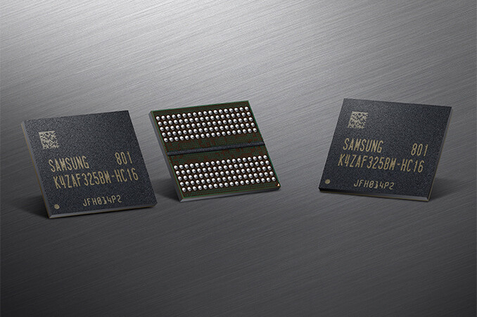
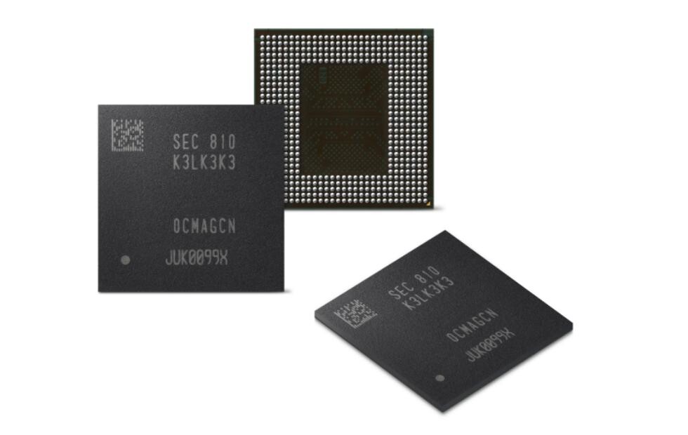
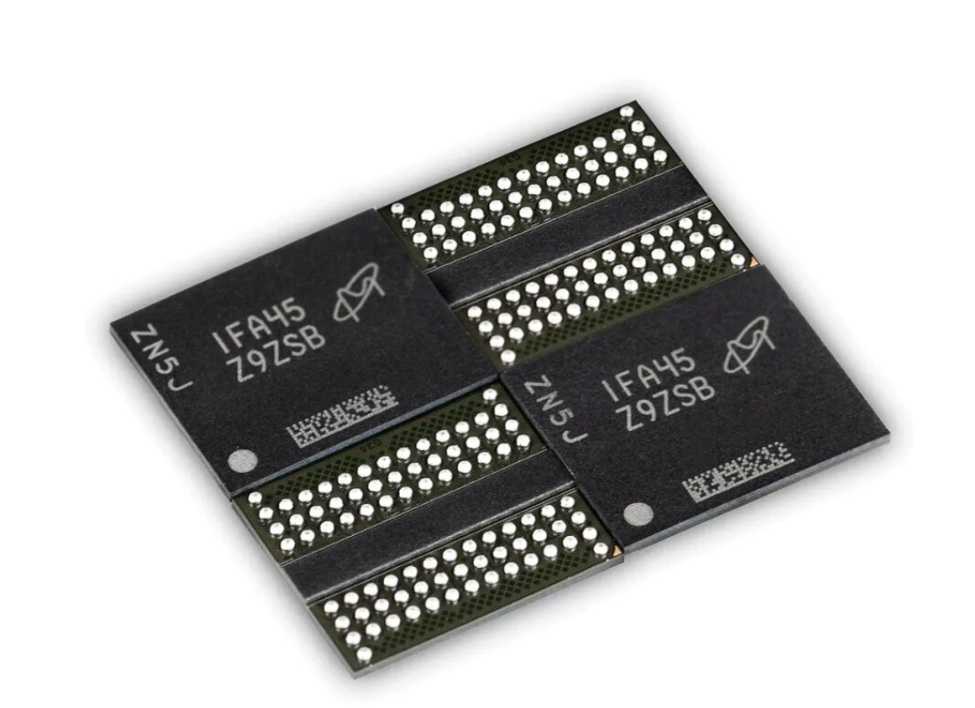
Micron Technology, Inc. announced today that MediaTek Inc. has validated Micron's low-power double data rate 5X (LPDDR5X) DRAM for MediaTek's new Dimensity 9000 5G flagship chipset for smartphones. Micron is the first semiconductor company to sample and validate this fastest, most advanced mobile memory in the industry and has shipped the first batch of samples of LPDDR5X built on its first-to-market 1α (1-alpha) node. Designed for high-end and flagship smartphones, Micron's LPDDR5X allows the smartphone ecosystem to unlock the next wave of data-intensive applications powered by artificial intelligence (AI) and 5G innovation.

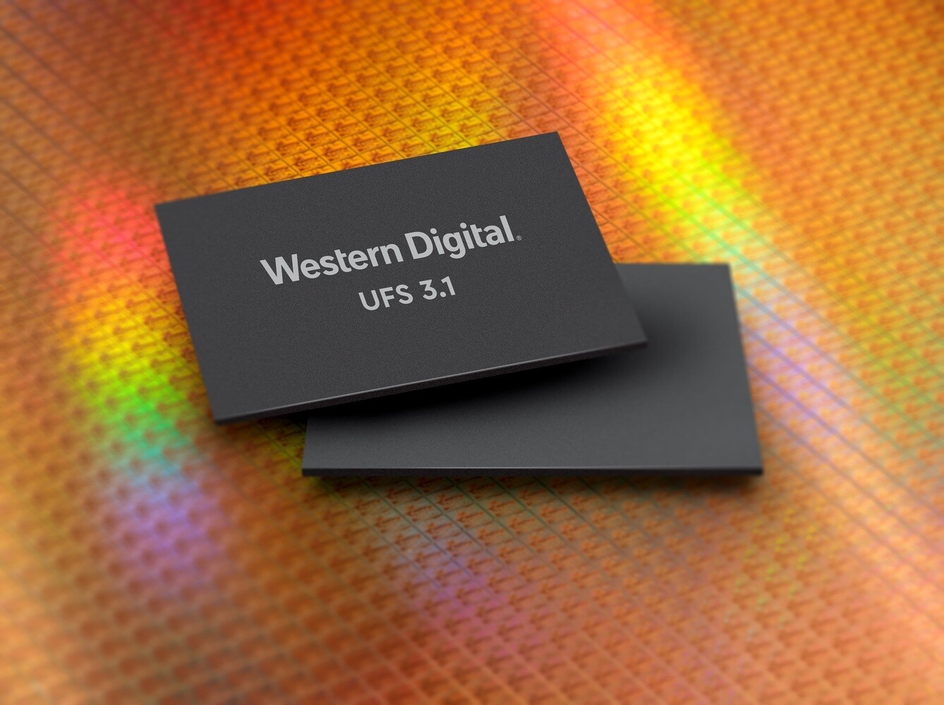
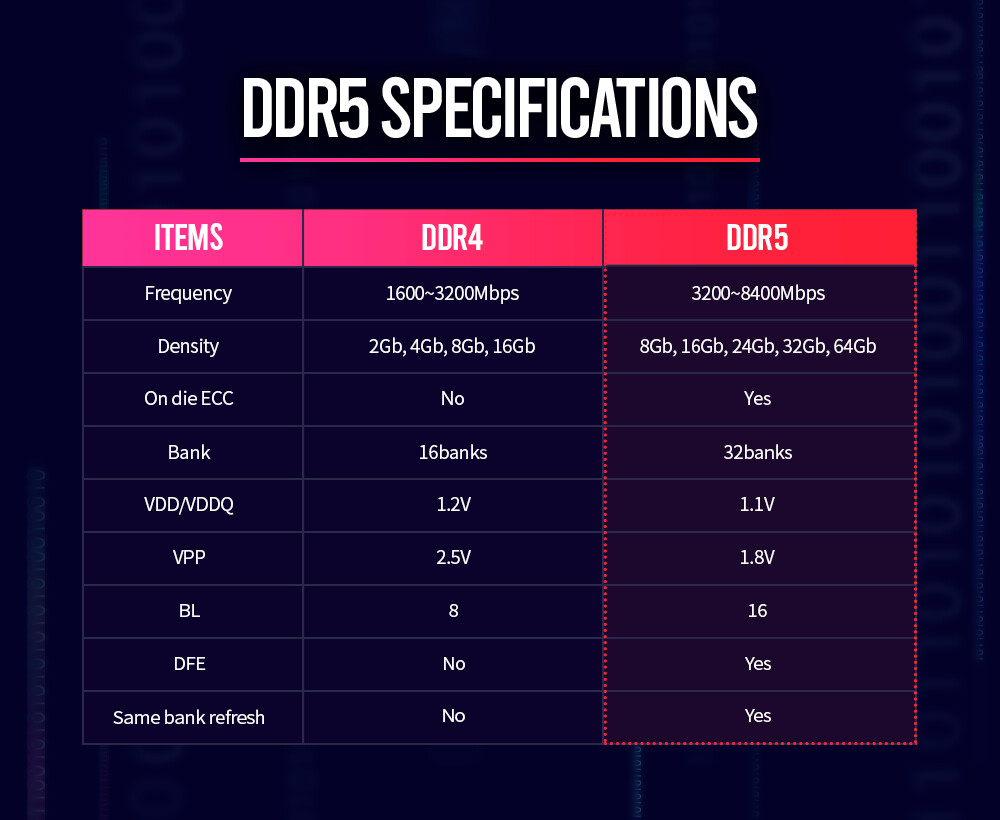
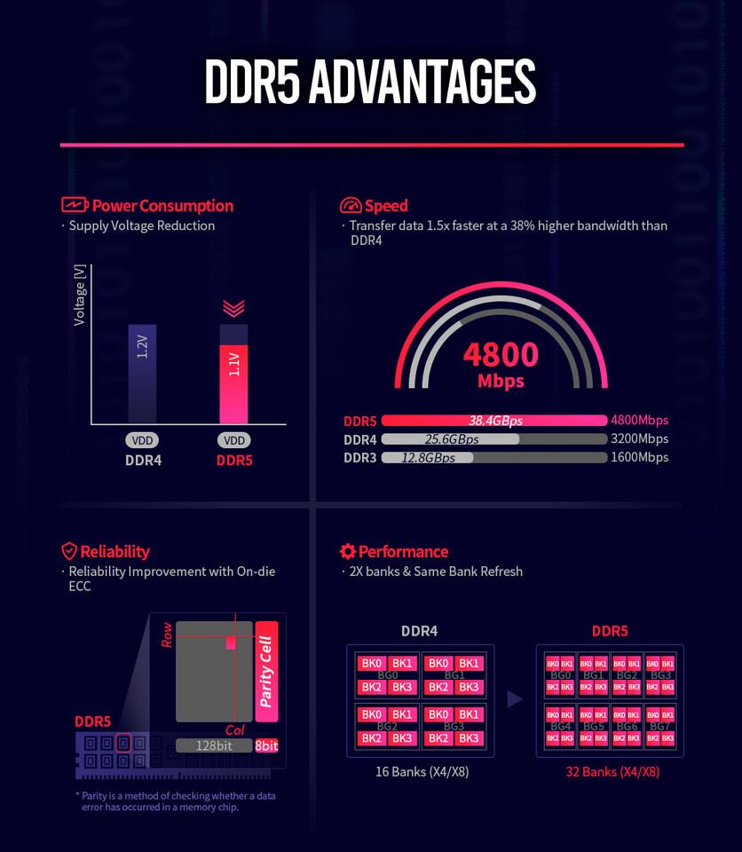
The market delivery and validation of Micron's industry-leading 1α-based LPDDR5X solidifies its product innovation and leadership in the mobile ecosystem, following industry-first launches for LPDDR5, 1α-based LPDDR4X, 176-layer NAND-based UFS 3.1 and uMCP5 solutions. This most recent milestone follows quickly on the heels of JEDEC's July release of the LPDDR5X extension to LPDDR5, created to offer higher bandwidth and memory speed for enhanced 5G communication and performance while still conserving power. Micron has validated samples supporting data rates up to 7.5 Gb/s, with samples supporting data rates up to 8.533 Gb/s to follow. Peak LPDDR5X speeds of 8.533 Gb/s deliver up to 33% faster performance than previous-generation LPDDR5.

"Innovating cutting-edge smartphone experiences requires memory technology built to address the massive bandwidth demands of the mobile market," said Raj Talluri, senior vice president and general manager of Micron's Mobile Business Unit. "Our collaboration with MediaTek to validate the world's most advanced mobile memory empowers the ecosystem to deliver the next wave of rich mobile features enhanced by 5G and AI."

Samsung Talks DDR6-12800, GDDR7 Development, and HBM3 Volume Production

During Samsung's Tech Day 2021, the company presented some interesting insights about the future of system memory technologies and how it plans to execute its production. Starting with the latest DDR5 standard, the company intends to follow JEDEC documents and offer some overclocking modules that surpass the specification advised by JEDEC. While the DDR5 standard specifies memory modules with 6,400 MT/s, Samsung will develop modules capable of overclocking up to 8,400 MT/s. These are not yet confirmed as they are still in the development phase. However, we can expect to see them in the later life of DDR5 memory.

The company also talked about the DDR6 standard, which is supposedly twice as fast as DDR5. The new DDR6 standard is still in early development, and all we know so far is that the number of memory channels per module is seeing a twofold increase over DDR5 to four channels. The number of memory banks also increases to 64. In addition to DDR6 for desktop and server use cases, the company is also working on Low Power DDR6 (LPDDR6) for mobile applications. While the company's LPDDR5 memory goes into volume production using the 1a-nm process at the beginning of 2022, the LPDDR6 is still in early development. The base speed for DDR6 modules will allegedly arrive at 12,800 MT/s, while overclocking modules will join the party at up to 17,000 MT/s. Mobile-oriented LPDDR6 version is also supposed to come with up to 17,000 MT/s speeds.

PNY Announces Specifications and Availability of XLR8 Gaming and Performance DDR5 Desktop Memory

PNY today announces specifications and availability for its upcoming Desktop Performance and XLR8 Gaming DDR5 memory products. The three models include the overclocked XLR8 Gaming MAKO and MAKO RGB models, running at 5600 MHz and a CAS latency of 36, as well as the PNY Performance model that follows JEDEC standards.

The XLR8 Gaming MAKO and MAKO RGB modules have been designed to meet the needs of gamers and enthusiasts. The designs for both modules feature aluminium heat spreaders with elements inspired by the powerful, fast and aggressive Mako shark from which they get their name. An XLR8 logo and GAMING text is proudly emblazoned on the side of the module and silver angled relief lines are machined into the heatspreader to reflect other components' lighting and provide unmatched flair and style.

JEDEC Publishes Update to DDR5 SDRAM Standard Used in HPC Applications

JEDEC Solid State Technology Association, the global leader in standards development for the microelectronics industry, today announced publication of the JESD79-5A DDR5 SDRAM standard. This update to the JEDEC DDR5 SDRAM standard includes features designed to enhance reliability and performance in a wide range of applications involving client systems and high-performance servers. JESD79-5A is now available for download from the JEDEC website.

Added features designed to meet industry demand for improved system reliability include bounded fault error-correction support, Soft Post-Package Repair (sPPR) undo and lock, Memory Built-In Self-Test Post Package Repair (MBIST and mPPR), Adaptive RFM, and an MR4 extension. JESD79-5A expands the timing definition and transfer speed of DDR5 up to 6400 MT/s for DRAM core timings and 5600 MT/s for IO AC timings to enable the industry to build an ecosystem up to 5600 MT/s. The nomenclature for core timing parameters and their respective definitions has been revamped to closely align with the upcoming JEDEC JESD400-5 DDR5 Serial Presence Detect (SPD) Contents V1.0 standard. The document can be accessed here.

ADATA Launches DDR5-4800 Memory Module

ADATA Technology, a manufacturer of high-performance DRAM modules, NAND Flash products, mobile accessories, gaming products, electric power trains, and industrial solutions today announces the ADATA DDR5-4800, a next-generation DDR5 memory module that is capable of reaching frequencies of up to 4800MT/s and comes with up to 32 GB of capacity. In addition, ADATA has worked with six major motherboard brands, including AORUS, ASROCK, ASUS, GIGABYTE, MSI and ROG to ensure optimal performance and compatibility across a wide range of motherboards.

"Through our strong R&D capabilities and close partnerships with the world's leading motherboard makers, we are committed to offering memory modules with next-generation performance, higher capacities, and enhanced stability," said Nick Dai, Senior Manager of DRAM Products at ADATA. "In the coming months, we will continue to launch a diverse array of DDR5 products to meet the different needs of creators, gamers, and other users."

JEDEC publishes XFM Embedded and Removable Memory Device Standard

JEDEC Solid State Technology Association, the global leader in standards development for the microelectronics industry, today announced the publication of JESD233: XFM Embedded and Removable Memory Device (XFMD) standard. XFMD (XFM stands for Crossover Flash Memory) is a new universal data storage media providing an NVMe over PCI Express interface in a small, thin form factor. The device is designed to bring replaceable storage to devices typically soldered down in IoT devices and embedded applications. Developed by JEDEC's JC-64.1 Subcommittee for Electrical Specifications and Command Protocols, JESD233 is available for download from the JEDEC website.

JESD233 XFMD is a removable, versatile memory solution intended for use in a wide range of applications that require an easy device exchange. Examples include IoT devices, automotive applications, notebook PCs, gaming consoles, video recording devices (drones, surveillance systems, etc.), Extended Reality (AR, VR, MR), and more.

To maximize connectivity between the host and the device, JESD233 XFMD leverages industry-leading standards from PCI-SIG and NVM Express, Inc. The PCI Express interface provides fundamental bus connectivity and NVM Express serves as the higher level protocol for accessing the non-volatile media as a low-latency logical storage device.

Neo Forza Details its DDR5 Memory Rollout Plan

PC enthusiast memory and storage brand Neo Forza, detailed its plans to roll out DDR5 memory for desktop PCs. It also sheds light on some of the possible combinations of memory speed and density under development. Q4 2021 is when the company's first DDR5 memory modules will debut. These will be basic, bare-PCB modules with specs and speeds closest to JEDEC's. The company will start out with DDR5-4800 MHz modules, with densities of 8 GB, 16 GB, and 32 GB. The starting CAS latency on these things appears to be 40T. From what we gather, 16 GB will be the new single-rank standard memory size, 8 GB single-rank will be a low-cost option; while 32 GB could be commonly dual-rank, rarely single-. These modules will likely be co-branded with authorized DRAM IC providers.

Vanilla DDR5-4800 modules are only the beginning. Neo Forza plans to develop gaming-grade memory modules, complete with chunky heatspreaders, RGB LED illumination, and more importantly, higher clock speeds. The company expects that as DDR5 matures as a standard, speeds of DDR5-6400, DDR5-7200, and DDR5-8600, will become common for the enthusiast segment. The higher frequency modules will likely be 16 GB single-rank. As densities ramp up, 64 GB dual-rank modules will be possible, and Neo Forza expects to ship 128 GB (2x 64 GB) dual-channel kits, or scale out to 4-channel thru 8-channel HEDT platforms.

JEDEC Publishes the New LPDDR5X Memory Standard

JEDEC Solid State Technology Association, the global leader in standards development for the microelectronics industry, today announced the publication of JESD209-5B, Low Power Double Data Rate 5 (LPDDR5). JESD209-5B includes both an update to the LPDDR5 standard that is focused on improving performance, power and flexibility, and a new LPDDR5X standard, which is an optional extension to LPDDR5.

Taken together, LPDDR5 and LPDDR5X are designed to significantly boost memory speed and efficiency for a variety of uses including mobile devices, such as 5G smartphones and artificial intelligence (AI) applications. Developed by JEDEC's JC-42.6 Subcommittee for Low Power Memories, JESD209-5B is available for download from the JEDEC website.

Western Digital Launches iNAND MC EU551 Storage for 5G Smartphones

Western Digital Corp. today announced its second-generation UFS 3.1 storage solution for 5G smartphones. The new Western Digital iNAND MC EU551 delivers the high-performance storage consumers need to be able to use their phones for emerging applications like ultra-high-resolution cameras, AR/VR, gaming and 8K video.

IDC expects 5G smartphone shipments to account for more than 40% of global volume in 2021 and grow to 69% in 2025. As networks continue to expand available bandwidth and offer lower latency to enable new user experiences, Western Digital's iNAND solutions deliver the high-capacity, high-performance embedded storage needed to power these exciting new applications.

Team Group Steps into the New DDR5 Era, Launches Team Elite DDR5 DIMM

At the end of 2020, TEAMGROUP reached a cooperation agreement with top DRAM wafer manufacturers and started working on DDR5 technology. Since then, TEAMGROUP has dedicated to the research and development of DDR5 modules, collaborating with various major motherboard manufacturers to ensure that each R&D stage undergoes comprehensive testing and to deliver products of the highest quality that the industry has ever seen. TEAMGROUP is leading the industry today as we announce our official launch of the world's first DDR5 memory module for desktops, the TEAMGROUP ELITE U-DIMM DDR5, which is estimated to be available on major EC platforms for consumers worldwide by the end of June and the beginning of July.

The initial launch of TEAMGROUP ELITE DDR5 memory module will support 16GBx2 of capacity at a frequency of 4800 MHz, with a voltage of 1.1 V CL40-40-40-77, which complies with the standard specifications defined by the JEDEC association. Compared to the maximum 3200 MHz standard frequency in the DDR4 generation, the DDR5 is able to increase the speed to up to 50%. The low 1.1 V voltage is also more energy efficient than its previous generation; to ensure minimum noise interference for the memory module, the power management is transferred from the motherboard onto the memory with an additional power management IC (PMIC) for more effective system load control. The most incredible feature of ELITE DDR5 is doubling the 16 banks of DDR4 to those of 32 in DDR5 to improve the IC structure, providing double access availability. An on-die ECC (error correction code) included in the DRAM IC is also available for self-recovery of the DRAM unit, ensuring that DRAM systems with DDR5 can obtain higher levels of stability.

Western Digital Unveils UFS 3.1 Compatible Embedded Flash Solutions

At its Flash Perspective Event today, Western Digital Corp. announced its new embedded flash platform for Universal Flash Storage (UFS) 3.1 to enable new applications in mobile, automotive, IoT, AR/VR, drones and other emerging segments that are reshaping the way we live, work and play.

In an increasingly mobile world of always on, always connected and always available, Western Digital's unique UFS 3.1 platform, based on the JEDEC-compliant UFS 3.1 specification, provides the speed, reliability and feature versatility that customers count on to build small, thin and lightweight solutions. Leveraging its vertical integration capability to optimize NAND, firmware, controller design, software and drivers, Western Digital can efficiently design purpose-built solutions for a variety of markets including mobile, IoT, automotive, and more - all leveraging a common UFS 3.1 architecture. Setting a new benchmark, this new platform is expected to deliver up to 90% improvement in sequential write performance, compared to its previous generation. This improvement will help realize 5G and Wi-Fi 6 download speed potential, delivering a better experience when consuming rich media files such as 8K video, as well as improved performance for applications such as burst mode photography.

CORSAIR Teases DDR5-6400 Memory Coming Later This Year

The fifth iteration of DDR technology, called DDR5, is set to arrive later this year. Many makers of DDR4 technology are announcing their plans to switch to the new standard, and CORSAIR is no exception. Known as the maker of high-quality products, CORSAIR has today posted a blog post teasing company's upcoming DDR5 products, and what they will be bringing to the table. For starters, the company has posted data about DDR5 modules that run at 6400 MHz speed, which is assumed to be the speed of the CORSAIR DDR5 modules when they arrive. At such speed, the memory can achieve a bandwidth of 51 GB/s, which is almost double the 26 GB/s that DDR4-3200 MHz memory achieves.

Another point CORSAIR wrote about is the capacity of a single DIMM. With DDR4, the company has made DIMMs that are only up to 32 GB in capacity. However, with DDR5, CORSAIR plans to quadruple that and build a single DDR5 DIMM that has up to 128 GB of memory on it. Another big point was the power required to run the new technology. The DDR4 standard required 1.2 Volts for operation, while the JEDEC specification says that DDR5 needs just 1.1 Volts to run. This will result in a cooler operation of memory modules.

Kingston Technology DDR5 Overclockable Modules One Step Closer to Reaching Market

Kingston Technology Company, Inc., a world leader in memory products and technology solutions, today announced it has sent overclockable DDR5 modules to its motherboard partners to begin qualification on the next-generation memory platform. Kingston engineered its DDR5 modules with a preset XMP profile, but also enabled our motherboard partners to manually adjust the power management integrated circuit (PMIC) beyond the 1.1 V DDR5 spec, thus allowing maximum flexibility to overclock. Kingston expects to ship its DDR5 solutions in Q3.

Memory validation requires cooperation of the entire computing ecosystem, and Kingston has forged close ties with the leading motherboard manufacturers and chipset makers throughout its 33-year history. This step continues the critical process of bringing leading high-performance and overclockable memory solutions to market later this year.

Netac Kickstarts Research and Development Process for 10 GHz DDR5 Memory

Netac, a Chinese company based in Shenzen claiming to be the inventor of USB flash drive, has reportedly started the research and development process of DDR5 memory modules that will outperform everything on the market. Netac is rumored to have started the development of DDR5 memory that will have a frequency of over 10,000 MHz. While the JEDEC specification notes that the DDR5 frequency range is between 4800-8400 MHz, manufacturers are always welcome to go over the official specifications. Being that Netac is a relatively new player in the PC memory space, we are wondering how the company plans to execute its plans.

A 10 GHz DDR5 memory would require a very high voltage to run, meaning high heat output. We know that DDR5 chips can run at 2.6 V, according to T-FORCE, who tested such a configuration earlier. The next potential problem would be a platform that could handle 10 GHz DDR5 memory, however, by the time we get this memory in our hands, platforms will mature enough to handle high-speed RAM. The first batch of new DDR5 memory that was sent to Netac was Micron's Z9ZSB modules, which are 2Gx8, CL40 memory modules. They are manufactured in the 1znm memory manufacturing node Micron uses. It is left to be seen what we end up with and if Netac delivers on its promise.

DDR5-6400 RAM Benchmarked on Intel Alder Lake Platform, Shows Major Improvement Over DDR4

As the industry is preparing for a shift to the new DDR standard, companies are trying to adopt the new technology and many companies are manufacturing the latest DDR5 memory modules. One of them is Shenzhen Longsys Electronics Co. Ltd, a Chinese manufacturer of memory chips, which has today demonstrated the power of DDR5 technology. Starting with this year, client platforms are expected to make a transition to the new standard, with the data center/server platform following. Using Intel's yet unreleased Alder Lake-S client platform, Longsys has been able to test its DDR5 DIMMs running at an amazing 6400 MHz speed and the company got some very interesting results.

Longsys has demoed a DDR5 module with 32 GB capacity, CAS Latency (CL) of 40 CL, operating voltage of 1.1 V, and memory modules clocked at 6400 MHz. With this being an impressive memory module, this is not the peak of DDR5. According to JEDEC specification, DDR5 will come with up to 8400 MHz speeds and capacities that are up to 128 GB per DIMM. Longsys has run some benchmarks, using an 8-core Alder Lake CPU, in AIDA64 and Ludashi. The company then proceeded to compare these results with DDR4-3200 MHz CL22 memory, which Longsys also manufactures. And the results? In AIDA64 tests, the new DDR5 module is faster anywhere from 12-36%, with the only regression seen in latency, where DDR5 is doubling it. In synthetic Ludashi Master Lu benchmark, the new DDR5 was spotted running 112% faster. Of course, these benchmarks, which you can check out here, are provided by the manufacturer, so you must take them with a grain of salt.

Chinese Manufacturer Asgard Launches 4,800 MHz DDR5 Memory Modules

In the name of Odin, Chinese manufacturer Asgard has launched their first DDR5 memory modules to market - beating some competing western companies that are still "gearing up" for it. Owned by the much less interestingly-named Shenzhen Jiahe Jinwei Electronic Technology Co., Ltd., Asgard likewise lost some of its flair in naming these DDR5 sticks - the best they could do was VMA5AUK-MMH224W3. The modules will be available in 32 GB, 64 GB and 128 GB per-stick densities.

The initial modules don't have any flair - they're built with the same green PCB that's actually the forerunner of today's colored ones. The company hs also announced that the modules win run at a relatively mild 4,800 MHz (the DDR5 specification goes up to 8,400 MHz), and that its timings coincide with JEDEC's "B" classification, which should mean 40-40-40. The voltage likewise remains at the JEDEC-set standard of 1.1 V. The company announced that mass-production rollout will only occur after there are actual CPUs and platforms that can take advantage of the DDR5 memory spec, and said that they expect Intel's Alder-Lake, Sapphire Rapids and Tiger Lake-U from the blue team, as well as Van Gogh and Rembrandt APUs from the AMD camp. No word on consumer pricing was available at time of writing.

JEDEC Publishes DDR4 NVDIMM-P Bus Protocol Standard

JEDEC Solid State Technology Association, the global leader in standards development for the microelectronics industry, today announced the publication of JESD304-4.01 DDR4 NVDIMM-P Bus Protocol. The JEDEC NVDIMM-P standard will enable the industry to create advanced memory solutions that benefit from the enhanced system performance and novel data availability offered by Persistent Memory devices. JESD304-4.01 DDR4 NVDIMM-P is available for download from the JEDEC website.

As demand for DRAM capacity and bandwidth continues to grow, Hybrid DIMM technologies such as NVDIMM-P provide an innovative method for attaching emerging Persistent Memory in computing systems. Combining the access speeds of DDR with the reliability and capacity of non-volatile memories gives design engineers a new approach to data management. Much more than a standard DIMM specification, NVDIMM-P provides a full transactional interface protocol compatible with standard DRAM DIMMs along with a firmware programming model for the modules. NVDIMM-P simultaneously maximizes both re-use and flexibility by minimizing system host changes, providing an interface of the lowest latency to emerging memory, and offering flexible support for varied Persistent Memory media characteristics and use cases.

ADATA Unveils Industrial-grade IEM5141A eMMC

ADATA Technology, a manufacturer of high-performance DRAM modules, NAND Flash products, mobile accessories, gaming products, electric power trains, and industrial solutions, today announces the ADATA IEM5141A embedded multi media cards. Ideally suited for industrial and IoT applications, the ADATA IEM5141A meets JEDEC eMMC 5.1 HS400 standard that delivers high read/write speeds of up to 300/170 MB/s,and low-power consumption of optimized performance.

The IEM5141A is a fully integrated device with built-in controllerand NAND Flash for higher capacities, durability, and perfectly suited for space-constrained IPCs and server boot-up applications. Furthermore, the IEM5141A offers Auto sleep on/off mode for low power consumption, Partitioning Management, and Thermal Throttling. It also features wide-temperature operability (-40°C - +85°C) and a 3,000 P/E cycle for excellent stability and reliability.

JEDEC Advances Universal Flash Storage (UFS) Removable Card Standard 3.0

JEDEC Solid State Technology Association, the worldwide leader in the development of standards for the microelectronics industry, today announced the publication of JESD220-2B Universal Flash Storage (UFS) Card Extension Standard 3.0. This new version of the removable memory card standard defines functionality closely aligned with the popular UFS 3.0 embedded device standard already widely recognized in many high-end mobile and consumer-focused applications. JESD220-2B is now available for download from the JEDEC website.

UFS is a prominent high-performance interface designed for use in applications where power consumption needs to be minimized, including mobile systems such as smartphones and tablets as well as for automotive and IOT applications. Its high-speed serial interface and optimized protocol enable major improvements in throughput and system performance.

TEAMGROUP is Taking the Global Lead in the New DDR5 Generation

As a world leader in computer memory, TEAMGROUP understands the importance of getting ahead in the next generation of DDR technology, hence it will be releasing ELITE series DDR5 memory in 2021. With over 20 years of experience developing DDR3 and DDR4 products, the company has dazzled the world with its advanced R&D capabilities and excellent product quality. After the JEDEC announced the DDR5 memory standard, TEAMGROUP has been actively designing and working together with our IC manufacturing partners to pioneer and prepare for this new generation.

TEAMGROUP is leading the way with its first DDR5 memory under its global top-selling ELITE memory product line. It plans to release a 16 GB 4800 MHz module operating at 1.1 V, down from the 1.2 V of the previous generation. The data transfer rate is increased to 4,800-5,200 Mbps, an increase of up to 1.6 times while reducing power consumption by 10%. Today's DDR4 memory with error correction code (ECC) requires an additional chip installed on the PCB, whereas DDR5 supports on-die ECC, a feature that self-corrects single-bit errors, greatly improving system stability. Anticipation is high for the efficiency improvements brought by the new generation, which can be utilized for big data and AI computing and other related applications.

Possible Radeon RX 6700 XT Specs Surface, 12GB the New Mid-Range Memory Size?

AMD could follow up on its RX 6800 series and RX 6900 XT launches with the RX 6700 series, which logically succeeds the RX 5700 series, and competes with NVIDIA's RTX 3060/Ti. Patrick Schur on Twitter, who has a high hit-rate with specs of upcoming AMD products, put out possible specs of the RX 6700 series. Both are based on the new "Navi 22" silicon, with an interesting set of specifications.

Apparently 12 GB could be AMD's new memory amount for the mid-range. It's unknown whether the 12 GB is running over a 192-bit wide memory interface (6x 16 Gbit chips), or whether AMD is using mixed-density chips over a 256-bit wide memory bus (think 4x 16 Gbit and 4x 8 Gbit), because even the fastest JEDEC-standard GDDR6 chips, running at 16 Gbps, would only yield 384 GB/s memory bandwidth, which is less than the 448 GB/s the RX 5700 series enjoy. Perhaps an Infinity Cache is deployed to make up the difference?

SK hynix Launches World's First DDR5 DRAM

SK hynix Inc. announced to launch world's first DDR5 DRAM. It is a high-speed and high-density product optimized for Big Data, Artificial Intelligence (AI), and machine learning (ML) as a next generation standard of DRAM. Since SK hynix announced the development of World's First 16 Gigabit (Gb) DDR5 DRAM on November 2018, the Company has provided its major partners including Intel with sample products, and has completed various tests and verification of its functions and compatibility. This will allow SK hynix to provide its customers with the products once the DDR5 market becomes active.

In the meantime, SK hynix has conducted joint-operation of on-site lab, system-level test, and simulation with System-on-Chip) (SoC) manufacturers to verify the functions of DDR5. Also, the Company validated compatibility of its DDR5 and the major components on DRAM module including register clock driver) (RCD), which affect DRAM performance, and power management integrated circuit) (PMIC). Through these verifications, SK hynix has been collaborating closely with its global partners.

JEDEC Publishes New DDR5 Standard for Advancing Next-Generation High Performance Computing Systems

JEDEC Solid State Technology Association, the global leader in the development of standards for the microelectronics industry, today announced the publication of the widely-anticipated JESD79-5 DDR5 SDRAM standard. The standard addresses demand requirements being driven by intensive cloud and enterprise data center applications, providing developers with twice the performance and much improved power efficiency. JESD79-5 DDR5 is now available for download from the JEDEC website.

DDR5 was designed to meet increasing needs for efficient performance in a wide range of applications including client systems and high-performance servers. DDR5 incorporates memory technology that leverages and extends industry know-how and experience developing previous DDR memories. The standard is architected to enable scaling memory performance without degrading channel efficiency at higher speeds, which has been achieved by doubling the burst-length to BL16 and bank-count to 32 from 16. This revolutionary architecture provides better channel efficiency and higher application level performance that will enable the continued evolution of next-generation computing systems. In addition, the DDR5 DIMM has two 40-bit fully independent sub-channels on the same module for efficiency and improved reliability.

New features, such as DFE (Decision Feedback Equalization), enable IO speed scalability for higher bandwidth and improved performance. DDR5 supports double the bandwidth as compared to its predecessor, DDR4, and is expected to be launched at 4.8 Gbps (50% higher than DDR4's end of life speed of 3.2 Gbps).

SK Hynix Unveils DDR5 Memory Details, Production to Start This Year

SK Hynix has today posted an update on their blog about the upcoming DDR5 memory, which they have developed in co-respondence with JEDEC's progression of the standard. They have noted a few key things, among which some of the most interesting are features like the maximum speed of 8400 Mbps. The DDR5 standard is very flexible, allowing manufacturers to release their chips with frequencies ranging anywhere from 3200-8400 Mbps. While the lowest speed is 3200 Mbps, manufacturers are starting with 4800 Mbps chips and building their way up from there. The minimum density of a single DDR5 die is 8 Gb, while the maximum is 64 Gb, quadrupling the maximum capacity of DDR4 dies.

Perhaps one of the biggest changes besides capacity and speed improvements is the addition of Error-Correcting Code (ECC) support for memory. This feature is now not exclusive to special dies, like with DDR4, but rather is built inside every die. The DDR5 memory chips use 32 banks, split into 8 bank groups, which is designed to provide as much bandwidth as possible. Burst Length is doubled to 16, compared to 8 of DDR4, so memory access availability is better. Operating Voltage is decreased to 1.1 V, from the previous 1.2 V of DDR4, resulting in an overall decrease of 20% of power consumption. The mass production of SK-Hynix's DDR5 chips will start this year, however, exact timing is unknown.
SK Hynix DDR5 SK Hynix DDR5 SK Hynix DDR5

DDR5 Arrives at 4800 MT/s Speeds, First SoCs this Year

Cadence, a fabless semiconductor company focusing on the development of IP solutions and IC design and verification tools, today posted an update regarding their development efforts for the 5th generation of DDR memory which is giving us some insights into the development of a new standard. The new DDR5 standard is supposed to bring better speeds and lower voltages while being more power-efficient. In the Cadence's blog called Breakfast Bytes, one of Cadence's memory experts talked about developments of the new standards and how they are developing the IP for the upcoming SoC solutions. Even though JEDEC, a company developing memory standards, hasn't officially published DDR5 standard specifications, Cadence is working closely with them to ensure that they stay on track and be the first on the market to deliver IP for the new standard.

Marc Greenberg, a Cadence expert for memory solutions was sharing his thoughts in the blog about the DDR5 and how it is progressing. Firstly, he notes that DDR5 is going to feature 4800 MT/s speeds at first. The initial speeds will improve throughout the 12 months when the data transfer rate will increase in the same fashion we have seen with previous generation DDR standards. Mr. Greenberg also shared that the goals of DDR5 are to have larger memory dies while managing latency challenges, same speed DRAM core as DDR4 with a higher speed I/O. He also noted that the goal of the new standard is not the bandwidth, but rather capacity - there should be 24Gb of memory per die initially, while later it should go up to 32Gb. That will allow for 256 GB DIMMs, where each byte can be accessed under 100 ns, making for a very responsive system. Mr. Greenberg also added that this is the year of DDR5, as Cadence is receiving a lot of orders for their 7 nm IP which should go in production systems this year.
Cadence DDR5
Return to Keyword Browsing
May 12th, 2024 09:26 EDT change timezone

New Forum Posts

Popular Reviews

Controversial News Posts