News Posts matching #NAND Memory

Return to Keyword Browsing

YMTC Develops 128 and 232-Layer Xtacking 4.0 NAND Memory Chips

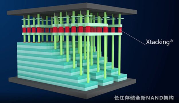
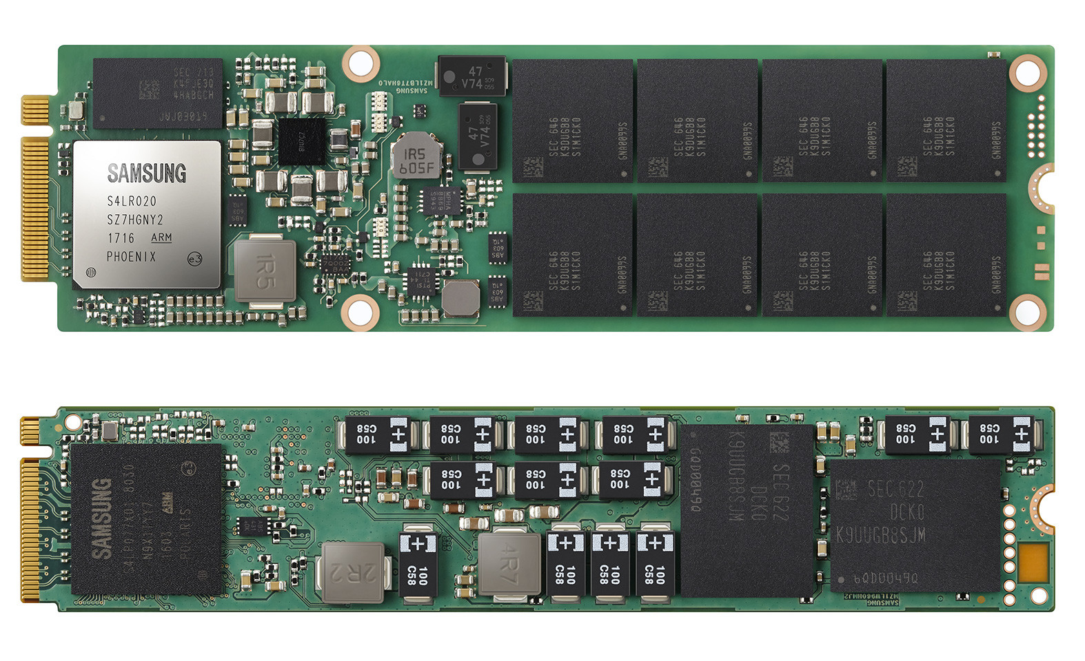
Chinese memory maker Yangtze Memory Technology Corp (YMTC) is allegedly preparing its next-generation Xtacking 4.0 3D NAND flash architecture for next-generation memory chips. According to the documentation obtained by Tom's Hardware, YMTC has developed two SKUs based on the upgraded Xtacking 4.0: X4-9060, a 128-layer three-bit-per-cell (TLC) 3D NAND, and the X4-9070, a 232-layer TLC 3D NAND. By using string stacking on both of these SKUs, YMTC plans to make the 3D NAND work by incorporating arrays with 64 and 116 active layers stacked on top of each other. This way, the export regulation rules from the US government are met, and the company can use the tools that are not under the sanction list.

While YMTC has yet to fully disclose the specific advantages of the Xtacking 4.0 technology, the industry anticipates significant enhancements in data transfer speeds and storage density. These improvements are expected to stem from increased plane counts for optimized parallel processing, refined bit/word line configurations to minimize latency, and the development of modified chip variants to boost production yields. When YMTC announced Xtacking 3.0, the company offered 128-layer TLC and 232-layer four-bit-per-cell (QLC) variants and was the first company to achieve 200+ layer count in the 3D NAND space. The Xtacking 3.0 architecture incorporates string stacking and hybrid bonding techniques and uses a mature process node for the chip's CMOS underlayer. We have to wait for the final Xtacking 4.0 details when YMTC's officially launches the SKUs.

JEDEC Updates Universal Flash Storage (UFS) and Supporting Memory Interface Standard

JEDEC Solid State Technology Association, the global leader in the development of standards for the microelectronics industry, today announced the publication of JESD220F: Universal Flash Storage 4.0. In addition, an update to the complementary JESD223E UFSHCI 4.0 standard, and a new companion standard for UFS version 3.1 and above, JESD231 File Based Optimization, have also been published. Developed for mobile applications and computing systems requiring high performance with low power consumption, UFS 4.0 introduces significant bandwidth and data protection improvements over the earlier version of the standard. All three standards are available for download from the JEDEC website.

NAND Flash Prices to Rise up to 40% in 2020

According to the sources over at DigiTimes, NAND flash prices are set to rise by up to 40% in 2020. This report is coming from sources over at memory chipmakers, presumably some of the biggest players like SK Hynix, Micron, and Samsung. If the prediction realizes, consumers will see a significant price jump for products based on NAND flash memory like most of today's solid-state drives. For reference, earlier today we also reported that a minute long power outage at Samsung created damage worth millions of Dollars in DRAM and NAND flash memory.

This incident alone could help contribute to the price rise of NAND memory in 2020. Other possible reasons may include an inefficient supply of materials used by NAND flash production lines or a simple supply-demand ratio, which would hurt prices of NAND flash long-therm. However, we hope that the underlying problems for this predicted price rise can be worked out and that companies like Samsung, which got power outage accident, can supplement the capacity loss during the unplanned turn of events.

Samsung to Double NAND Memory Output Capacity in China

Samsung Electronics has announced last Wednesday that they are planning to double their NAND memory output capacity in china. The announcement, done at a groundbreaking ceremony in its Xi'an fabrication facility in inland Shaanxi Province, should see some $7 billion invested over the course of three years. With this investment in both facilities and machinery, Samsung expected production capacity to roughly double from current values to some 220,000, 300 mm 3-D flash memory wafers by 2020.

The motives for this increased Samsung investment in mainland China are being put forward as a way for the South Korean giant to temper relationships with China, one of its greatest importers of NAND memory. Further investment into China likely assuages the country's protectionist policies, since at least it receives something back from its import volume. By investing further into a second assembly line at its Xi'an fabrication facility, Samsung is also looking to reduce risk derived from over-condensed manufacturing facilities in South Korea.

Micron and Intel Announce Update to NAND Memory Joint Development Program

Micron and Intel today announced an update to their successful NAND memory joint development partnership that has helped the companies develop and deliver industry-leading NAND technologies to market. The announcement involves the companies' mutual agreement to work independently on future generations of 3D NAND. The companies have agreed to complete development of their third-generation of 3D NAND technology, which will be delivered toward the end of this year and extending into early 2019. Beyond that technology node, both companies will develop 3D NAND independently in order to better optimize the technology and products for their individual business needs.

Micron and Intel expect no change in the cadence of their respective 3D NAND technology development of future nodes. The two companies are currently ramping products based on their second-generation of 3D NAND (64 layer) technology. Both companies will also continue to jointly develop and manufacture 3D XPoint at the Intel-Micron Flash Technologies (IMFT) joint venture fab in Lehi, Utah, which is now entirely focused on 3D XPoint memory production.

Samsung Introduces Far-reaching V-NAND Memory Solutions

Samsung Electronics, the world leader in advanced memory technology, has announced new V-NAND (Vertical NAND) memory solutions and technology that will address the pressing requirements of next-generation data processing and storage systems. With the rapid increase of data-intensive applications across many industries using artificial intelligence and Internet of Things (IoT) technologies, the role of flash memory has become extremely critical in accelerating the speed at which information can be extracted for real-time analysis.

At the inaugural Samsung Tech Day and this year's Flash Memory Summit, Samsung is showcasing solutions to address next-generation data processing challenges centered around the company's latest V-NAND technology and an array of solid state drives (SSDs). These solutions will be at the forefront of enabling today's most data-intensive tasks such as high-performance computing, machine learning, real-time analytics and parallel computing.

Samsung Ramps up 64-Layer 3D V-NAND Memory Production

Samsung Electronics, the world leader in advanced memory technology, today announced that it has begun volume production of 64-layer, 256Gb V-NAND flash memory for use with an expanding line-up of storage solutions for server, PC and mobile applications. Since Samsung began producing the industry's first SSD based on 64-layer 256Gb V-NAND chips in January for key IT customers, it has been working on a wide range of new V-NAND-based mobile and consumer storage solutions. These include embedded UFS memory, branded SSDs and external memory cards, which the company plans to introduce later this year.

To solidify its competitive edge in the memory market, Samsung intends for its volume production of the 64-layer V-NAND chip, which is widely referred to as 4th generation V-NAND, to cover more than 50 percent of its monthly NAND flash production by year end. "Following a long commitment to innovative technology, we will continuously push the limits of generations of industry-first V-NAND production, in moving the industry closer to the advent of the terabit V-NAND era," said Kye Hyun Kyung, Executive Vice President of the Flash Product and Technology team, Memory Business at Samsung Electronics. "We will keep developing next-generation V-NAND products in sync with the global IT industry so that we can contribute to the timeliest launches of new systems and services, in bringing a higher level of satisfaction to consumers."

Intel and Micron develop first-ever 128 Gb NAND Flash memory chip

Flash buddies Intel and Micron have today announced a significant breakthrough in terms of NAND density, the first 128 Gb (16 GB) MLC NAND memory chip. Manufactured on 20 nm process technology, this 128 Gb chip complies with the ONFI 3.0 specification (enabling speeds of up to 333 megatransfers per second) and can be used for new, high-capacity solid state drives, as well as for next-generation tablets, smartphones and other portable devices.

According to Intel and Micron, this milestone was made possible by the use of a new, innovative cell structure that 'breaks the scaling constraints of the standard NAND floating gate cell by integrating the first Hi-K/metal gate stack on NAND production.'

Samsung Introduces High-speed 512GB SSD Utilizing New Toggle-mode DDR NAND Memory

Samsung Electronics Co., Ltd., the world leader in advanced semiconductor technology solutions, today introduced the first solid state drive (SSD) utilizing high-performance toggle-mode DDR NAND. The new 512 gigabyte (GB) SSD provides electronic data processing application designers with advanced performance and reliability for notebooks with premium value.

"The highly advanced features and characteristics of our new SSD were obtained as a direct result of an aggressive push for further development of our NAND flash technology, our SSD controller and our supportive SSD firmware," said Dong-Soo Jun, executive vice president, memory marketing, Samsung Electronics. "Early introduction of this state-of-the-art toggle DDR solution will enable Samsung to play a major role in securing faster market acceptance of the new wave of high-end SSD technology," he added.

Hynix, Numonyx and Phison Join to Develop NAND Memory System Solutions

Hynix Semiconductor Inc, Numonyx B.V. and Phison Electronics Corp. today announced that they have signed a collaboration agreement to jointly develop controllers for the next generation of managed-NAND solutions based on the newly released JEDEC eMMC 4.4 industry specification. The collaboration is expected to speed the delivery of the industry's most advanced eMMC specification available, helping to manage and simplify high-capacity storage requirements and improve the overall system-level performance of wireless and embedded applications.
Under this agreement, Phison, Hynix and Numonyx will leverage their respective competencies to develop controllers used in combination with a variety of NAND flash products. Phison will exclusively supply the jointly developed controllers to Hynix and Numonyx, which will enhance their respective NAND flash memory solutions portfolio.

Micron to Cut 15% of its Workforce During the Next Two Years

After reporting a $344 million fourth-quarter loss last week Micron today said it is going to reduce its global workforce by approximately 15 percent during the next two years. Most of the workforce cuts will occur in Boise.
The combination of declining customer demand and product oversupply in the marketplace has driven selling prices for NAND flash memory significantly below manufacturing costs,
Micron said in a statement.
As a result, IM Flash Technologies (IMFT), a joint venture between Micron and Intel, will discontinue the supply of NAND flash memory from Micron's Boise facility. The NAND operation shutdown will reduce IMFT's NAND flash production by approximately 35,000 (200 millimeter) wafers per month, according to Micron. Production in the other two joint ownership NAND flash facilities in Lehi and Utah will continue operating at full speed for now.

Intel, STMicroelectronics and Francisco Partners Close Transaction to Create Numonyx

Intel Corporation today announced that the company has finalized and closed its transaction with STMicroelectronics and Francisco Partners to create a new independent semiconductor company Numonyx B.V. that will design, develop and manufacture NOR and NAND flash memory products. As part of the transaction, Intel has transferred the assets associated with its NOR flash memory business and certain assets related to the company's phase change memory initiatives to Numonyx in exchange for 45.1 percent ownership in Numonyx. ST Microelectronics acquired a 48.6 percent ownership interest in Numonyx. Francisco Partners acquired a 6.3 percent ownership interest in exchange for a cash investment of $150 million.

Intel and Micron Develop the World’s Fastest NAND Flash Memory

Intel Corporation and Micron Technology today unveiled a high speed NAND flash memory technology that can greatly enhance the access and transfer of data in devices that use silicon for storage. The new technology - developed jointly by Intel and Micron and manufactured by the companies' NAND flash joint venture, IM Flash Technologies (IMFT) - is five times faster than conventional NAND, allowing data to be transferred in a fraction of the time for computing, video, photography and other computing applications.

AMD Licenses NAND Flash System Solution From Denali

Denali Software, a world-leading provider of electronic design automation (EDA) software and intellectual property (IP), today announced it has licensed its NAND Flash solution to AMD. Per this agreement, AMD is licensing Denali Databahn NAND Flash controller and Spectra flash file system for inclusion in next-generation processors for handheld devices, providing high performance, simplified system development and low development cost benefits to handheld manufacturers.

Samsung and Toshiba to Share Specifications for Premium NAND Flash

Samsung Electronics and Toshiba announced today that they have signed a cross-license deal to produce, market and sell memory with the specifications and trademarks of Samsung's OneNAND and Toshiba's LBA-NAND memory chips. The arrangement is expected to result in increased availability of premium-performance OneNAND and LBA-NAND flash devices worldwide. Under the terms of the agreement, Samsung will license product specifications of its integrated OneNAND and Flex-OneNAND "fusion" memory chips to Toshiba, while Toshiba will license product specifications of its single-package LBA-NAND and mobileLBA-NAND flash chips to Samsung. Both companies will develop and market products that are compatible with the respective original-source technology. Samsung and Toshiba each plan to release products next year based on the respectively licensed product specifications, according to the companies.

ONFi Announces ONFi 2.0 Specification for NAND Devices

The Open NAND Flash Interface (ONFi) Working Group, the organization dedicated to simplifying integration of NAND Flash memory into consumer electronic (CE) devices, computing platforms and industrial systems, today announced the availability of the 0.9 draft of the ONFi 2.0 specification to member companies. This signals the imminent release of the ONFi 2.0 specification in January 2008. With 71 member companies supporting ONFi development, this scaleable technology secures its foothold in the industry.
Return to Keyword Browsing
Apr 26th, 2024 07:37 EDT change timezone

New Forum Posts

Popular Reviews

Controversial News Posts