News Posts matching #Semiconductor

Return to Keyword Browsing

GlobalFoundries and ON Semi Partner to Transfer Ownership of East Fishkill NY 300mm Fab

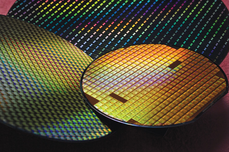
ON Semiconductor Corporation and GLOBALFOUNDRIES today announced that they have entered into a definitive agreement for ON Semiconductor to acquire a 300 mm fab located in East Fishkill, New York. The total consideration for the acquisition is $430 million, of which $100 million has been paid at signing of the definitive agreement, and $330 million will be paid at the end of 2022, after which ON Semiconductor will gain full operational control of the fab, and the site's employees will transition to ON Semiconductor. Completion of the transaction is subject to regulatory approval and other customary closing conditions.

The agreement allows ON Semiconductor to increase its 300 mm production at the East Fishkill fab over several years, and allows for GLOBALFOUNDRIES to transition its numerous technologies to the company's three other at-scale 300 mm sites. Under the terms of the agreement, GLOBALFOUNDRIES will manufacture 300 mm wafers for ON Semiconductor until the end of 2022. First production of 300 mm wafers for ON Semiconductor is expected to start in 2020.

Toshiba Consolidates Two of its Semiconductor Subsidiaries

Toshiba Electronic Devices & Storage Corporation (TDSC) today announced the consolidation of two of its subsidiaries, Toshiba Microelectronics Corporation (TOSMEC) and Toshiba Discrete Semiconductor Technology Corporation (TDIT), into a new company, Toshiba Electronic Device Solutions Corporation (TEDS). The move is expected to strengthen capabilities in proposing solutions and bringing greater efficiency to R&D for the semiconductor business. TEDS will start operation on April 1.

TDIT's business covers product development and technical sales for discrete semiconductors, while TOSMEC provides comprehensive services for system LSI, ranging from product planning, development and design to testing and failure analysis. Following the merger, TEDS will be responsible for product planning, product development, failure analysis and solution proposals for the semiconductor business, and will cooperate with TDSC as the engineering arm of its semiconductor business.

China-based SMIC to Start Manufacture of 14 nm-class Chips in 2H 2019

As R&D costs for new, smaller manufacturing nodes grow at unprecedented rates across the industry, a new player is set to enter the 14 nm process manufacture competition: China-based SMIC (Semiconductor Manufacturing International Corporation). The company is looking to throw its hat on the lucrative 14 nm process, filling its offerings portfolio under the 28 nm it currently offers as its denser process.

The company expects its 95% yield rate to offer its customers a trusted platform that might help it increase revenue for further investment on its 10 nm and 7 nm EUV nodes, which the company is pursuing (despite other industry veterans, such as former AMD-manufacturing arm GLOBALFOUNDRIES having ceased development on). Manufacturing technology that's competitive with the western world's, and that's developed in-country, is paramount for China's intention of reducing its dependence of foreign technology, which is why this is such a big step for the company and the company's aspirations.

TSMC Cleared to Build New 3 nm Manufacturing Factory in Southern Taiwan

The world's largest contract semiconductor manufacturing company, TSMC, has been cleared to commence construction of a new 3 nm chip factory at the Southern Taiwan Science Park in Tainan. The new factory is expected to use 20 percent renewable energy and 50 percent recycled water.

The factory's environmental impact assessment was accepted by the Environmental Protection Administration (EPA) on Dec. 19, after concerns were raised about use of water and power sources. TSMC is expected to invest NT$600 million (US$19.45 million) in the project, with construction to begin in 2022. Production is planned to start in late 2022 or early 2023. At the same site, TSMC is also building a 5 nm chip factory, which is expected to be up and running in late 2019 or early 2020.

It Does Matter How You Spin it - Spintronics Could be Answer to Future Semiconductor Technologies

It's only a matter of time before microchip production as we know it disappears entirely, at least for leading-edge tech designs. Either via new materials applied to trusted techniques (such as carbon coating/nanotubes) or entirely new and exotic fabrication technologies, we're rapidly approaching the limits of traditional silicon-based microchips. One solution to the problem, as it stands, might be found in spintronics - an interesting concept which bases processing and data retention not simply on whether current is being applied to a given transistor (as is the case for current silicon chips), but on a property of electrons called spin. Crucially, changing the magnetic orientation of electrons requires but a single charge, instead of a continued supply of power - which allows for much lower power consumption and heat output, two of the encroaching, limiting factors for the usual chips.

AMD President and CEO Dr. Lisa Su Bestowed with GSA Exemplary Leadership Award

Global Semiconductor Alliance (GSA) will honor industry visionary and innovator Dr. Lisa Su, President and CEO, Advanced Micro Devices (AMD), with the prestigious Dr. Morris Chang Exemplary Leadership Award at its highly-anticipated Annual Awards Dinner to be held in Santa Clara, California, on December 6, 2018.

Established in 1999, the Dr. Morris Chang Exemplary Leadership Award recognizes individuals for their exceptional contributions, exemplifying how their vision and global leadership have transformed and elevated the entire semiconductor industry. The selection of Dr. Su is based on her ongoing technological contributions, exceptional business acumen, status as a positive and inspiring role model, and wide ranging respect among the technology industry and business community.

Samsung Unveils 256-Gigabyte 3DS DDR4 RDIMM, Other Datacenter Innovations

Samsung Electronics, a world leader in advanced semiconductor technology, today announced several groundbreaking additions to its comprehensive semiconductor ecosystem that encompass next-generation technologies in foundry as well as NAND flash, SSD (solid state drive) and DRAM. Together, these developments mark a giant step forward for Samsung's semiconductor business.

"Samsung's technology leadership and product breadth are unparalleled," said JS Choi, President, Samsung Semiconductor, Inc. "Bringing 7 nm EUV into production is an incredible achievement. Also, the announcements of SmartSSD and 256GB 3DS RDIMM represent performance and capacity breakthroughs that will continue to push compute boundaries. Together, these additions to Samsung's comprehensive technology ecosystem will power the next generation of datacenters, high-performance computing (HPC), enterprise, artificial intelligence (AI) and emerging applications."

Rollercoaster Monday for AMD as it Loses Jim Anderson, Closes Above $25 in Stock Price

It has been a rollercoaster Monday for AMD as it bled yet another bright executive. Jim Anderson, who led Computing and Graphics Group after the departure of Raja Koduri, and who is rumored to have conceived the idea of Threadripper and the client-segment monetization of the "Zen" architecture, left AMD to become CEO of Lattice Semiconductor, a company that designs FPGAs. Anderson will be paid an inducement award of company shares valued up to $2.9 million.

On the same day, AMD stock crossed $25 to close at $25.26 up 5.34 percent, a historic high since way back in 2006 as Intel was beginning to regain its footing with its Core processor family. This raises the company's market cap to $22.9 billion. AMD is better funded than ever (in over 12 years), to start a new GPU project, for example. CTO Mark Papermaster, in a company blog post assured customers that AMD is going all-in with 7 nanometer, and it could bank more heavily on TSMC to achieve its roadmap goals of first-to-market 7 nm CPU and GPU by end of the year.

Samsung Introduces High-Density 6Gbps SATA SSD and 16Gb-64GB DDR4 RDIMM

Samsung Electronics Co., Ltd., the world leader in advanced memory technology, today announced that it is rolling out its PM883, the highest density datacenter SATA drive, at eight terabytes (TB). Samsung's new solid state drive (SSD) offering is the industry's first datacenter SATA drive to incorporate LPDDR4 DRAM modules and features a 6.0-gigabits-per-second (Gbps) 2.5-inch SATA interface.

The high-performance PM883 is expected to accelerate a transition in many existing enterprise datacenters to SATA-formatted SSD designs, with improved economies of scale through the use of advanced-generation V-NAND technology at higher densities.

"We are thrilled to have the opportunity to enable a high level of storage density with low power consumption, which thanks to the efficiency of our 64-layer V-NAND-based technology, allows us to double the capacity of current SATA storage," said Jim Elliott, corporate senior vice president, memory sales and marketing, Samsung Semiconductor, Inc. "Our expanded lineup for the PM883 will offer up to 8TB to allow optimal use in existing enterprise and cloud storage systems."

Samsung to Invest $27.7 billion On Second Pyeongtaek Semiconductor Plant

Samsung's management committee has reportedly convened this morning, February 7th, to officially approve an investment plan on a new semicondctor manufacturing facility. Reports say this new factory is expected to be built on Pyeongtaek, the same general location as Samsung's current Pyeongtaek Fab 1. The investment plan is being made with plans for the plant to start production of the "P2-Project" plant during the first half of 2019.

Giving credence to these industry reports is the fact that Samsung has already celebrate gas pipeline contracts with companies (such as Wonik Holdings), just last month, in preparation for this new fab construction. It's as of yet unclear what specific plan the company has for the new factory, though it will certainly inject extraordinary new amounts of volume to Samsung's various foundry businesses. With two years of construction since it broke ground in May, 2015, the original fabrication line at the Pyeongtaek campus is currently the largest single Fab in the industry; in the face of this, it seems that a "first half of 2019" starting date for semiconductor production at Samsung's new manufacturing facilities may be slightly optimistic. However, those plans start to sound a little more on the doable side if one considers these might actually be plans for an expansion of the current Pyeongtaek Fab 1 facilities, plans for which the company has already announced back in July 2017.

Samsung Electronics Announces Fourth Quarter and FY 2017 Results

One of the industry's giants is having a strong showing, with a grand total of $64.17 billion in revenue and $14 billion in profits for Q4 2017. These results were buoyed by earnings increases across almost all of Samsung's sectors: the Consumer Electronics, Device Solutions, and Display Panel sectors registered strong growth. The only outlier was IT & Mobile Communications, where the company fell short for the second consecutive quarter (likely has something to do with splash damage from Samsung's still too close for comfort, exploding failures).

Samsung is expecting stable NAND demand alongside increased DRAM demand for datacenters. Samsung is citing "strong market conditions" for its semiconductor revenue (particularly considering DRAM pricing and volume), and says that what would be, under normal circumstances, a slow quarter due to low seasonality of its semiconductor business was somewhat compensated by Samsung's acquisition of new China clients (I wonder if this has anything to do with mining ASICs...) There's also no mention of Samsung's entry into the OLED TV market, with the company instead choosing to focus on its Quantum Dot technology, higher resolution panels, and higher diagonals as the method of choice to attract new buyers. The full press release follows.

AMD To Change Suppliers for Vega 20 GPUs on 7nm, HBM2 Packaging for Vega 11

AMD's RX Vega supply has seen exceedingly limited quantities available since launch. This has been due to a number of reasons, though the two foremost that have been reported are: increased demand from cryptocurrency miners, who are looking towards maximizing their single node hashrate density through Vega's promising mining capabilities; and yield issues with AMD's Vega 10 HBM2 packaging partner, Advanced Semiconductor Engineering (ASE). It's expected that chip yield for Vega 10 is also lower per se, due to it having a 484 mm² die, which is more prone to defects than a smaller one, thus reducing the amount of fully-enabled GPUs.

AMD's production partner, GlobalFoundries, has historically been at the center of considerations on AMD's yield problems. That GlobalFoundries is seemingly doing a good job with Ryzen may not be much to say: those chips have incredibly small die sizes (192 mm²) for their number of cores. It seems that Global Foundries only hits problems with increased die sizes and complexity (which is, unfortunately for AMD, where it matters most).

Toshiba and WD Power Struggle Continues - WD Bid for Toshiba's Business 6 Times

You must remember the ongoing house of horrors that is Toshiba's financial situation. Granted, it isn't that bad - the company is still managing to push the envelope on its semiconductor production business. Still, I'm sure the company would have liked to not be on the verge of selling out 20% of its memory business production stake - which is one of the company's most profitable divisions to begin with.

TSMC to Build New $15.7 Billion Fab in Taiwan, for 3 nm and 5 nm Chips

TSMC (Taiwan Semiconductor Manufacturing Co.), one of the foremost semiconductor producers in the world - which controls a leading 55% share of the global market - said on Wednesday it plans to build a new, $15.7 billion facility in Taiwan that would churn out 5 nm and 3 nm chips. If TSMC were to achieve these production nodes in a timely fashion (with "timely" meaning "before their competitors"), that would prove a huge boon for the company, as everyone - and especially deep-pocketed smartphone chip designers such as Apple and Qualcomm - is looking towards evolution in process nodes, which allows for improvements in power consumption, performance, size and cost of chips per wafer.

"We're asking the government to help us find a plot that is large enough (123 to 197 acres) and has convenient access so we can build an advanced chip plant to manufacture 5 nm and 3 nm chips," TSMC spokesperson Elizabeth Sun said. The spokesperson declined to provide details about the timing of the construction and production, though it's seemingly still a few years away (yet close enough for it to merit an official request). TSMC co-CEO Mark Liu had already mentioned that the company was working on 5 nm chips, and had assigned the task of developing 3 nm technology and conducting research on 2 nm technology to upwards of 300 engineers. Delays on EUV (Extreme Ultraviolet) lithography have slowed expected advancements in further miniaturization of the process nodes. It remains to be seen which technology TSMC is counting on towards aiding them in their goals for 5 nm, 3 nm and the mentioned 2 nm chip production, especially since at those sizes, we start leaving the usual realm of plane old physics, crossing the threshold towards their exotic cousins, quantum physics.

Toshiba Launches Client SSDs Using 15nm TLC NAND Flash Memory

Toshiba Corporation's Semiconductor & Storage Products Company today announced the launch of the "SG5 series" of client SSDs integrating NAND chips fabricated with 15nm TLC process technology. The new products, which include high capacity 1024GB models, will be available in 2.5-type and M.2 2280 (single- and double-sided) form factors, to meet various mounting requirements from the expansion of SSD application fields. Sample shipments start from today.

The SG5 series is equipped with Toshiba's proprietary QSBC (Quadruple Swing-By Code) error correction technology, a highly efficient error correction code (ECC) which helps protect customer data from corruption and improves reliability. Toshiba will continue strengthening its SSD lineup, meeting the various needs of users and leading the continuously expanding SSD market.

Vivante to Highlight Cutting-Edge GraphiVisor Virtualization Technology

Vivante Corporation today announces that its GPU GraphiVisor solution will be featured in a white paper and sponsorship at the Jon Peddie Research Virtualize Conference. GraphiVisor is at the heart of solutions that must be both high-performance and secure, such as in Automotive applications, where feature-rich user experiences must exist in the same system as safety-critical functions with no tolerance for error or tampering. GraphiVisor will work alongside traditional security measures such as 2-step authentication, encryption and network security for truly secure systems in applications where some systems must be designed to have uninhibited, immediate access to the GPU and even a small error-margin is unacceptable, and a new level of hardware isolation is necessary. Vivante IP provides that option with two GPUs that can operate in isolation on one system.

Vivante is excited to be a part of the 2015 Virtualize Conference, with a best practices panel on virtualization options that will include Rick Tewell of Freescale Semiconductor, who heads the Graphics Architecture team for the i.MX product lines. Freescale has adopted Vivante's dual-GPU isolation technology in the i.MX6 Quad to allow one Microcontroller solution for multiple graphics applications that have varying requirements for safety and real-time performance.

TSMC to Commence 10 nm Volume Production by Q4-2016

Semiconductor foundry TSMC assured its clients that the company will be ready with a 10 nanometer manufacturing node for volume production, by the 4th quarter of 2016. Company president and joint-CEO Mark Liu made this announcement during the company's recent Q2-2015 earnings call. "The recent progress of our 10 nanometer technology development is very encouraging and on track with our plan," he said. With volume production of chips commencing in Q4, some of the first products based on them should begin appearing in early-2017. "We ramp up 10 nm in the Q4 2016 next year, but the real product shipment will be in Q1 2017," said C.C. Wei, co-CEO.

New Micron "Ultra" Memory Products Enable Next-Generation Automotive Systems

Micron Technology, Inc., today announced the availability of ultra reliable, ultra high-speed and ultra high-temperature parallel NOR Flash and low-power DDR4 (LPDDR4) DRAM to meet the increasing memory requirements for the automotive market segment. Micron's G18 NOR family offers the industry's highest-performance parallel NOR, while Micron's automotive-grade LPDDR4 solutions are an industry-first.

These new products meet the needs of automotive applications that require ultra high speed. The G18 family's high performance (266 MB/s)enables faster boot and code execution for higher-density applications, while LPDDR4 enables 33 percent higher peak bandwidth than DDR4. Additionally, Micron's new solutions deliver long-lasting reliability and meet ISO/TS certification requirements-with the G18 family enabling three times faster throughput over quad SPI NOR, and the LPDDR4 products undergoing additional package-level burn-in testing. Furthermore, Micron's G18 NOR products have options that meet the industrial temperature (IT) range of -40 to 85°C and the automotive-grade automotive temperature (AAT) range of -40 to 105°C. The LPDDR4 products have options that meet the automotive-grade industrial temperature (AIT) range of -40 to 95°C, as well as some future options that will meet the automotive-grade ultra temperature (AUT) range of -40C to 125°C, which is the highest operating temperature range in the industry, expected to be available in 2016.

Toshiba and SanDisk Celebrate the Opening of the Second Phase of Fab 5

Toshiba Corporation and SanDisk Corporation today celebrated the opening of the second phase of the No. 5 semiconductor fabrication facility (Fab 5) and the start of construction of the new No. 2 fabrication facility (Fab 2) at Yokkaichi Operations, Toshiba's NAND Flash memory plant in Mie prefecture, Japan.

Toshiba started construction of the second phase of Fab 5 in August 2013, and Toshiba and SanDisk have overseen installation of production equipment in the expanded facility since July this year. Production in phase 2 began at the start of this month, with 15 nm NAND flash memory process technology, the world's smallest and most advanced node. Toshiba and SanDisk announced deployment of this jointly developed 15 nm NAND flash process in April this year, with initial production in part of Fab 5 phase 1, and now target conversion of the remaining capacity in phase 1 to the new process technology.

GLOBALFOUNDRIES Names Tom Caulfield as GM of its New York Fab

GLOBALFOUNDRIES, a leading provider of advanced semiconductor manufacturing technology, today appointed Dr. Thomas Caulfield as senior vice president and general manager of the company's latest leading-edge 300mm semiconductor wafer manufacturing facility (Fab 8), located in Saratoga County, NY. Caulfield, an accomplished industry leader with more than 20 years of technical and global executive experience, will lead the operations, expansion and ramp of semiconductor manufacturing production at Fab 8, where GLOBALFOUNDRIES supports customers on the world's most advanced semiconductor manufacturing technology platforms including 28 nanometer (nm), 20 nm, and the recently announced 14 nm FinFET platform.

"We are expanding our Fab 8 manufacturing campus, strengthening strategic partnerships, and deepening customer relationships so we can offer our customers leading-edge technology and a more flexible and cost-effective way of doing business," said GLOBALFOUNDRIES CEO Sanjay Jha. "Tom is a proven and respected industry leader with more than two decades of semiconductor technology and manufacturing experience and we are excited to have him join our team to drive the next phase of growth at Fab 8."

Toshiba Joins GLOBALSOLUTIONS Ecosystem as Worldwide ASIC Partner

GLOBALFOUNDRIES today announced that Toshiba Corporation will join the company's GLOBALSOLUTIONS ecosystem of partners. As a worldwide ASIC partner, Toshiba will enable its Fit Fast Structured Array (FFSA) and ASIC solutions based upon GLOBALFOUNDRIES' technologies and services for customers across the globe. The agreement includes participation on multi-project wafer (MPW) runs and production wafers covering the whole portfolio of GLOBALFOUNDRIES technologies, including leading-edge process nodes.

Initially, the partnership will focus on implementations of Toshiba's FFSAs manufactured with GLOBALFOUNDRIES' 65nm and 40nm low-power process technologies, with 28nm arrays to follow. Toshiba's FFSA products-including libraries and intellectual property (IP)-allow customers to reduce development time and costs by customizing existing base wafers, choosing from a number of design platforms at GLOBALFOUNDRIES. For higher-volume applications, customers can work with Toshiba's libraries to develop fully custom system-on-chips (SoCs). With an initial product completed, customers can then leverage the embedded FFSA technology to provide quick-turn derivative products, with much lower development costs.

Toshiba to Collaborate with GLOBALFOUNDRIES on FFSA Manufacturing

Toshiba Corporation today announced that the company will collaborate with GLOBALFOUNDRIES in the manufacture of Toshiba's FFSA (Fit Fast Structured Array) products. Toshiba will expand its FFSA business through production at GLOBALFOUNDRIES's fabs. Initial products will be manufactured using GLOBALFOUNDRIES 65nm-LPe and 40nm-LP processes, with plans to extend the collaboration to the company's 28nm High-K Metal Gate (HKMG) technology.

Toshiba's FFSA products, developed in collaboration with BaySand Inc. of the U.S., can be configured simply by customizing the design of a few metal layers. This customization process secures a much shorter development turn-around-time than with conventional ASIC devices, and satisfies increasing market needs for high performance, high specifications and low power technologies. At a time of ever-shorter product life cycles, time available for development is at a premium, and solutions that meet demand and allow tweaking of the specifications until just before the start of trial production increase the freedom and flexibility of developers.

Micron Technology Appoints Rajan Rajgopal as Vice President of Quality

Micron Technology, Inc. (Nasdaq:MU), today announced that the company has named Rajan Rajgopal, vice president of Quality. Rajgopal will be responsible for overseeing all aspects of Micron's quality systems including manufacturing, customer program management and product ramps. He brings more than 25 years of experience to Micron and most recently served as the vice president of Global Quality and Customer Enablement for GLOBALFOUNDRIES in Singapore.

"Micron continues to evolve as a memory business driven by systems-level solutions, and quality plays a heightened role in serving our valued customers," said Micron President Mark Adams. "We are excited to have Rajan join our team and leverage his experience in serving our customers in an increasingly diversified set of application segments."

Toshiba Expands its Semiconductor Facility at Yokkaichi

Toshiba Corporation today announced that it will expand its state-of-art No. 5 semiconductor fabrication facility (Fab 5) at Yokkaichi Operations in Mie, Japan, to secure manufacturing space for NAND flash memories fabricated with next generation process technology and for future 3D memories. Fab 5 second phase construction will start at the end of August this year and be completed in summer next year. Decisions on equipment investment and production will reflect market trends.

Yokkaichi Operations currently has three Fabs mass producing NAND flash memory, including Fab 5 phase 1. Fab 5's construction was planned around two phases, the first of which went into operation in July 2011. After giving careful consideration to the balance of product supply and demand, and noting a recovery driven by growing demand for smartphones, tablets, SSD for enterprise servers and other new applications, Toshiba now anticipates further medium- to long-term market expansion and recognizes that the time is right to expand Fab 5.

UMC joins IBM chip alliance for 10 nm process development

IBM (NYSE: IBM) and United Microelectronics Corporation (NYSE: UMC; TWSE: 2303) ("UMC"), a leading global semiconductor foundry, today announced that UMC will join the IBM Technology Development Alliances as a participant in the group's development of 10nm CMOS process technology.

"Established over a decade ago, the IBM alliance allows the partners to leverage our combined expertise and collaborative research and innovative technology development to address the demanding needs for advanced semiconductor applications," said Gary Patton, VP, IBM Semiconductor Research & Development. "UMC is a strong addition to the alliance."
Return to Keyword Browsing
May 19th, 2024 12:47 EDT change timezone

New Forum Posts

Popular Reviews

Controversial News Posts