News Posts matching #Semiconductor

Return to Keyword Browsing

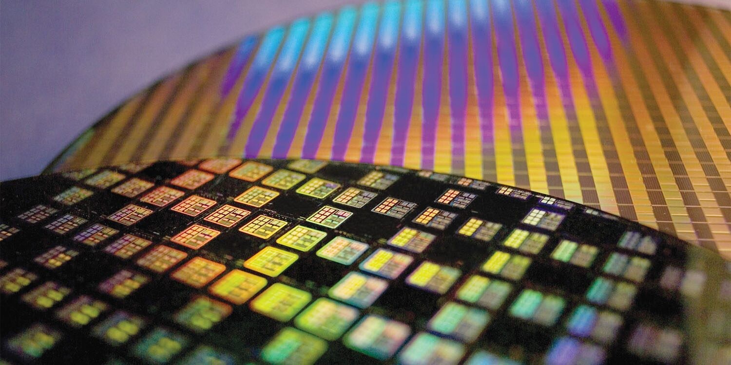
Samsung's 5 nm EUV Node Struggles with Yields

Semiconductor manufacturing is a difficult process. Often when a new node is being developed, there are new materials introduced that may cause some yield issues. Or perhaps with 7 nm and below nodes, they are quite difficult to manufacture due to their size, as the transistor can get damaged by the smallest impurity in silicon. So manufacturers have to be extra careful and must spend more time on the development of new nodes. According to industry sources over at DigiTimes, we have information that Samsung is struggling with its 5 nm EUV node.

This unfortunate news comes after the industry sources of DigiTimes reported that Qualcomm's next-generation 5G chipsets could be affected if Samsung doesn't improve its yields. While there are no specific pieces of information on what is the main cause of bad yields, there could be a plethora of reasons. From anything related to manufacturing equipment to silicon impurities. We don't know yet. We hope that Samsung can sort out these issues in time, so Qualcomm wouldn't need to reserve its orders at rival foundries and port the design to a new process.

TSMC Becomes the Biggest Semiconductor Company in the World

Taiwan Semiconductor Manufacturing Company, called TSMC shorty, has just become the world's biggest semiconductor company. The news broke after TSMC's stock reached a peak heights of $66.40 price per share, and market capitalization of 313 billion US dollars. That means that the Taiwanese company officially passed Intel, NVIDIA, and Samsung in terms of market capitalization, which is no small feat. And the news isn't that surprising. TSMC has been rather busy with orders from customers, just waiting for new spots so they can grab a piece of its production pipeline.

TrendForce, a market intelligence provider, estimates that TSMC has an amazing 51.9% of global semiconductor foundry share alone. That is no small feat but TSMC worked hard over the years to make it happen. With constant investments into R&D, TSMC has managed to make itself not only competitive with other foundries, but rather an industry leader. With 5 nm already going in high-volume manufacturing (HVM) in Q4 of this year, the company is demonstrating that it is the market leader with the latest node developments. Smaller nodes like 3 nm are already in development and TSMC doesn't plan to stop.
TSMC HQ

SMIC Makes a Debut on China STAR Market

Chinese silicon manufacturer Semiconductor Manufacturing International (SMIC) has officially made a debut on the Chinese science and technology innovation board (STAR) as of today. After submitting a proposal 16 days ago, SMIC already managed to start trading its shares on the STAR board of China's Shanghai Stock Exchange (SSE). Why this is important you might wonder? Well now SMIC can collect more funds and invest that into node development, so the Chinese semiconductor industry is about to boom. Being the biggest semiconductor manufacturer in China, SMIC takes the lead and every development from the company is big for the Chinese semiconductor industry.

SMIC is currently trading on the Stock Exchange of Hong Kong (HKEX) where it used to trade exclusively. With SSE now included, it is easier for the company to trade. SMIC also submitted a proposal last year in May to start trading on the New York Stock Exchange (NYSE) so it can get the attention of Western investors. If the company manages to successfully raise all the funds for node development, then the Chinese semiconductor industry is about to flourish.

Analog Devices Acquires Maxim Integrated

Analog Devices, Inc. (Nasdaq: ADI) and Maxim Integrated Products, Inc. (Nasdaq: MXIM) today announced that they have entered into a definitive agreement under which ADI will acquire Maxim in an all stock transaction that values the combined enterprise at over $68 billion. The transaction, which was unanimously approved by the Boards of Directors of both companies, will strengthen ADI as an analog semiconductor leader with increased breadth and scale across multiple attractive end markets.

Under the terms of the agreement, Maxim stockholders will receive 0.630 of a share of ADI common stock for each share of Maxim common stock they hold at the closing of the transaction. Upon closing, current ADI stockholders will own approximately 69 percent of the combined company, while Maxim stockholders will own approximately 31 percent. The transaction is intended to qualify as a tax-free reorganization for U.S. federal income tax purposes.

Samsung Leads Semiconductor Paradigm Shift with New Material Discovery

Researchers at the Samsung Advanced Institute of Technology (SAIT) have unveiled the discovery of a new material, called amorphous boron nitride (a-BN), in collaboration with Ulsan National Institute of Science and Technology (UNIST) and the University of Cambridge. Published in the journal Nature, the study has the potential to accelerate the advent of the next generation of semiconductors.

Recently, SAIT has been working on the research and development of two-dimensional (2D) materials - crystalline materials with a single layer of atoms. Specifically, the institute has been working on the research and development of graphene, and has achieved groundbreaking research outcomes in this area such as the development of a new graphene transistor as well as a novel method of producing large-area, single-crystal wafer-scale graphene. In addition to researching and developing graphene, SAIT has been working to accelerate the material's commercialization.

Lattice Semiconductor Announces Certus-NX General Purpose FPGA

Lattice Semiconductor Corporation, the low power programmable leader, today launched the new Lattice Certus -NX family of FPGAs. The devices lead the general-purpose FPGA market in I/O density, delivering up to twice the I/O density per mm2 in comparison to similar competing FPGAs, and provide best-in-class power savings, small size, reliability, instant-on performance, and support fast PCI Express (PCIe) and Gigabit Ethernet interfaces to enable data co-processing, signal bridging, and system control. Certus-NX FPGAs target a range of applications, from data processing in automated industrial equipment to system management in communications infrastructure. The Certus-NX devices are the second family of FPGAs developed on the Lattice Nexus platform, the industry's first low power FPGA platform using 28 nm FD-SOI process technology. With the launch of Certus-NX, Lattice marks the release of the second device family developed under Lattice's new product development strategy in just six months.

"Certus-NX delivers unique and innovative capabilities that set it apart," said Linley Gwennap, Principal Analyst at The Linley Group. "Compared to competing FPGAs of similar gate counts, Lattice offers a much smaller package, greater I/O density, and lower power."

Intel Plans to Volume Manufacture Nanowire/Nanoribbon Transistors in Five Years

Semiconductor manufacturing is a hard business. There is a constant need for manufacturers to compete with each other and if they don't, they get left behind. Intel, as one of the biggest semiconductor makers in the world, is always trying to invent new technologies spending massive R&D funds on semiconductors. New technologies such as nanowire/nanoribbon transistors, which are supposed to enable transistor sizes unimaginable now, are on its way to make it in the hand of consumers. During the international VLSI conference, Intel's CTO Mike Mayberry held a presentation about how Intel plans to address the demand for more compute by showing off new technologies.

With a presentation titled "The Future of Compute", Mr. Mayberry made some exciting claims and predictions. So far, we have been used to FinFET transistors since the 22 nm node from Intel. However, as nodes get smaller the gate of the transistor is not enough to keep it from switching randomly. So to avoid that problem Intel, along with other semiconductor manufacturers like Samsung, created a solution called Gate-All-Around FET (GAAFET). This technology takes a transistor fin and wraps in around all sides (see picture below), so the gate has better switching control, preventing random switching and errors. As a fin, nanowire or nanosheet (wider option from nanowire) can be used and they can be stacked. These allow for additional control of tailoring whatever a node will be used for high performance or low power. Intel predicts that they will start high volume manufacturing of silicon based on this technology in five years. This is setting an important milestone for Intel as well as other industry players, as now everyone will rush to deliver it first. It is now a waiting game to see who will actually come out with it first.
Intel Nanowire/Nanoribbon Samsung GAAFET

Semiconductor Fabs to Log Record Spending of Nearly $68 Billion in 2021, SEMI Reports

2021 is poised to mark a banner year for global fab equipment spending with 24 percent growth to a record US$67.7 billion, 10 percent higher than the previously forecast US$65.7 billion, and all product segments promising solid growth rates, according to the second-quarter 2020 update of the SEMI World Fab Forecast report. Memory fabs will lead worldwide semiconductor segments with US$30 billion in equipment spending, while leading-edge logic and foundry is expected to rank second with US$29 billion in investments.

The 3D NAND memory subsegment will help power the spending spree with a 30 percent jump in investments this year before tacking on 17 percent growth in 2021. DRAM fab investments will surge 50 percent next year after declining 11 percent in 2020, and fab spending on logic and foundry, mainly leading edge, will trace a similar but more muted trajectory, rising 16 percent 2021 after an 11 percent drop this year.

Samsung Receives Zero Waste to Landfill Validations for All of its Semiconductor Manufacturing Sites

Samsung Electronics Co., Ltd., a world leader in advanced semiconductor technology, today announced that it has received UL's Zero Waste to Landfill validation of Gold level and above for all of its global semiconductor operation sites. This signifies that Samsung's semiconductor sites in South Korea, US and China meet the requirement of more than 95-percent waste diversion through methods that do not involve thermal processing. In particular, the Samsung DSR building in Hwaseong, Korea, home to most of its local semiconductor R&D staff, is validated for Zero Waste to Landfill at the Platinum level for reaching 100-percent waste diversion.

"The Zero Waste to Landfill Gold validation is testament to the care and effort by our employees around the world to protect the environment," said Chanhoon Park, executive vice president of global infrastructure technology at Samsung Electronics. "Eco-friendly operations are now a must for any business and we will continue to ensure sustainable growth that is mindful of the environment that we live and operate in."

Teledyne e2v Introduces First Radiation-Tolerant DDR4 Memory for Space Applications

Teledyne e2v has announced the DDR4T04G72M - the first radiation-tolerant DDR4 memory chip, featuring a total 4 GB capacity. Currently validated at 2133 MT/s, and targeting to offer 2400MT/s in the near future, this next-generation solution offers ultra-responsive low latency operation, while fitting into a highly compact form factor. Furthermore, high-reliability manufacturing and radiation-tolerant robustness makes it highly suitable for dealing with the rigors of space environments.

With 15 mm x 20 mm x 1.92 mm dimensions, this new space-grade device comprises an array of Micron based memory chips, integrated in a single package. It features a 72-bit bus, where 64 bits are dedicated to data and 8 bits to error correction code (ECC). Radiation tests have been performed on these memory chips and a single event effects (SEE) report is available from Teledyne e2v. In particular, the memory has been demonstrated to be single event latch-up (SEL) free up to 60+ MeV.cm²/mg.

Researchers Propose New Density Metric for Semiconductor Technology

In today's world, fabrication process identification of semiconductor technology has become little more than marketing fluff. Whereas not that long ago, fabrication processes could (mostly) be directly compared on the basis of transistor density (ie, 300 nm, 32 nm, 14 nm, and now 7 nm), recent advances in manufacturing technologies and their end terminology have lost all significance when it comes to actually describe how density that process is. The way manufacturers measured this semiconductor density used to directly refer to the minimum gate length in transistors fabricated in a given process - that, is, in 300 nm, the minimum gate length that could be achieved was 300 nanometers, in 32 nm, 32 nanometres, and so on. As of now, that isn't happening - which is why we've got Intel saying that its 10 nm fabrication process will be comparable to TSMC's current 7 nm process.

This leads to a number of difficulties for interested parties to actually glean any meaningful information from this particular semiconductor metric alone. Now, a team of researchers has tackled this problem by suggesting a different way to express semiconductor manufacturing capability. Their intention is to allow to "gauge advances in future generations of semiconductor technologies in a holistic way, by accounting for the progress in logic, memory, and packaging/integration technologies simultaneously." As such, their proposed density metric follows a [DL, DM, DC] philosophy, where DL is the density of logic transistors (in #/mm²), DM is the bit density of main memory (currently the off-chip DRAM density, in #/mm²), and DC is the density of connections between the main memory and logic (in #/mm²). The researchers say that current top semiconductor technology density available would be described by this system as [38M, 383M, 12K].

Intel Regains Top Position in Semiconductor Market

Intel has regained its position of semiconductor leader by revenue from Samsung for the 2019 period. Intel had been trailing Samsung for the last 2 years but after a decline in DRAM demand Intel reclaimed the leading position. The overall semiconductor market saw revenue drops of 12% in 2019 which hit other companies worse than Intel.

Andrew Norwood, research VP at Gartner says: "Oversupply in the DRAM market helped push the overall memory market down 32.7% 2019. The memory market accounted for 26.1% of semiconductor sales in 2019 and was the worst-performing device segment,". Samsung being a large DRAM supplier was hit hard by this compared to Intel with limited memory production. Gartner the research firm has also cut its global semiconductor market outlook this year to a 0.9% dip from the 12.5% growth estimated at the end of 2019 due to the effects of COVID-19.

Huawei Moves 14 nm Silicon Orders from TSMC to SMIC

Huawei's subsidiary, HiSilicon, which designs the processors used in Huawei's smartphones and telecommunications equipment, has reportedly moved its silicon orders from Taiwan Semiconductor Manufacturing Company (TSMC) to Semiconductor Manufacturing International Corporation (SMIC), according to DigiTimes. Why Huawei decided to do is move all of the 14 nm orders from Taiwanese foundry to China's largest silicon manufacturing fab, is to give itself peace of mind if the plan of the US Government goes through to stop TSMC from supplying Huawei. At least for the mid-tier chips built using 14 nm node, Huawei would gain some peace as a Chinese fab is a safer choice given the current political situation.

When it comes to the high-end SoCs built on 7 nm, and 5 nm in the future, it is is still uncertain how will Huawei behave in this situation, meaning that if US cuts off TSMC's supply to Huawei, they will be forced to use SMIC's 7 nm-class N+1 node instead of anything from TSMC. Another option would be Samsung, but it is a question will Huawei put itself in risk to be dependant on another foreign company. The lack of 14 nm orders from Huawei will not be reflecting much on TSMC, because whenever someone decides to cut orders, another company takes up the manufacturing capactiy. For example, when Huawei cut its 5 nm orders, Apple absorbed by ordering more capacity. When Huawei also cut 7 nm orders, AMD and other big customers decided to order more, making the situation feel like there is a real fight for TSMC's capacity.
Silicon Wafer

Gartner Forecasts Worldwide Semiconductor Revenue to Decline 0.9% in 2020 Due to Coronavirus Impact

Due to the impact of the coronavirus on semiconductor supply and demand, worldwide semiconductor revenue is forecast to decline 0.9% in 2020, according to Gartner, Inc. This is down from the previous quarter's forecast of 12.5% growth.

"The wide spread of COVID-19 across the world and the resulting strong actions by governments to contain the spread will have a far more severe impact on demand than initially predicted," said Richard Gordon, research practice vice president at Gartner. "This year's forecast could have been worse, but growth in memory could prevent a steep decline."
Gartner WorldWide Semiconductor Revenue Forcast

SMIC 7nm-class N+1 Foundry Node Going Live by Q4-2020

China's state-backed SMIC (Semiconductor Manufacturing International Corporation) has set an ambitious target of Q4-2020 for its 7 nanometer-class N+1 foundry node to go live, achieving "small scale production," according to a cnTechPost report. The company has a lot of weight on its shoulders as geopolitical hostility between the U.S. and China threatens to derail the country's plans to dominate 5G technology markets around the world. The SMIC N+1 node is designed to improve performance by 20%, reduce chip power consumption by 57%, reduce logic area by 63%, and reduce SoC area by 55%, in comparison to the SMIC's 14 nm FinFET node, Chinese press reports citing a statement from SMIC's co-CEO Dr. Liang Mengsong.

Dr. Liang confirmed that the N+1 7 nm node and its immediate successor will not use EUV lithography. N+1 will receive a refinement in the form of N+2, with modest chip power consumption improvement goals compared to N+1. This is similar to SMIC's 12 nm FinFET node being a refinement of its 14 nm FinFET node. Later down its lifecycle, once the company has got a handle of its EUV lithography equipment, N+2 could receive various photomasks, including a switch to EUV at scale.

TSMC to Hire 4000 new Staff for Next-Generation Semiconductor Node Development

TSMC is set to hire about 4000 new staff members to gain a workforce for its development of next-generation semiconductor manufacturing nodes. The goal of the company is to gather talent so it can develop the world's leading semiconductor nodes, like 3 nm and below. With 15 billion USD planned for R&D purposes alone this year, TSMC is investing a big part of its capital back into development on new and improved technology. Markets such as 5G and High-Performance Computing are leading the charge and require smaller, faster, and more efficient semiconductor nodes, which TSMC plans to deliver. To gather talent, TSMC started job listing using recruitment website TaiwanJobs and started campaigns on university campuses to attract grad students.

TrendForce: The Effect of the Covid-19 Corona Virus Measured on Tech Industry

The following analysis shows TrendForce's investigations of key component and other downstream technology industries, under the impact of the COVID-19 outbreak, with the latest data as of February 14, 2020.

Semiconductors
Compared to the OSAT industry, the foundry industry has a much higher degree of fab automation and thus is less impacted by the outbreak. But because most workers at semiconductor manufacturing sites in China come from out of town, labor shortages and traffic restrictions will lower work resumption rates at foundries more than expected. In the short term, fab utilization rates may not make a full recovery. As a result, given that the outbreak has not yet been effectively contained, TrendForce is projecting a possible decline in shipment for the Chinese foundry industry in 1Q20, in turn affecting downstream Chinese OSAT companies. The industry's overall performance recovery remains to be seen.

Arm Delivers New Edge Processor IPs for IoT

Today, Arm announced significant additions to its artificial intelligence (AI) platform, including new machine learning (ML) IP, the Arm Cortex -M55 processor and Arm Ethos -U55 NPU, the industry's first microNPU (Neural Processing Unit) for Cortex-M, designed to deliver a combined 480x leap in ML performance to microcontrollers. The new IP and supporting unified toolchain enable AI hardware and software developers with more ways to innovate as a result of unprecedented levels of on-device ML processing for billions of small, power-constrained IoT and embedded devices.

Minute-long Power Outage at Samsung Plant Damages Millions Worth DRAM and NAND

A tiny minute-long power-outage halted production at a Samsung Electronics plant in Hwaseong, South Korea, according to a Reuters report citing Korean news agency Yonhap. This stopped some production lines of DRAM and NAND flash memory. A source with "direct knowledge of the matter" told Reuters that the outage likely caused millions of Dollars in losses to Samsung. Semiconductor manufacturing in general is a very power-sensitive process, and a stoppage at any of its manufacturing stages can result in wasted batches; not to mention the time lost to recovery. For instance, a 30-minute power outage in 2018 inflicted a $43.32 million loss to Samsung.

The cause of the power outage on Tuesday afternoon (31st December), is said to be a fault with a regional transmission cable. It will take Samsung up to two days (mid-Thursday) to get the production line rolling again. On the flipside, the resulting drop in output could help Samsung push out its swelling NAND flash and DRAM inventory, reports Yonhap, citing an analyst.

TSMC Becomes Asia's Most Valuable Company

Taiwan Semiconductor Manufacturing Company, Limited, also known as TSMC shortly became Asia's biggest and the most valuable company with a market cap of over 8.02 trillion New Taiwan Dollars, which roughly translates to 262.75 billion US Dollars. Becoming the biggest Asian company, TSMC's market capitalization has now surpassed Samsung for the first time in the history of company existence.

The underlying reasons for becoming a company that TSMC is today, are plenty. Firstly, they are providing customers with the flexibility of choosing any manufacturing node, whatever it is the latest 7 nm or the older ones like 180 nm. They have a choice whatever they want to use something older and less expensive or something newer for high-performance and lower power. Additionally, TSMC is re-investing a big part of its profits into research and development efforts to stay competitive and deliver only the best technology to its customers, on time.

Panasonic Exits Silicon Manufacturing Business

Panasonic, an electronics manufacturing giant, has today sold its silicon manufacturing business, marking the end of an era of Japanese semiconductor manufacturing. Once a big player in silicon manufacturing scene, particularly in the '80s and '90s era when Japan's silicon output was huge, Panasonic was considered one of the main players in the silicon manufacturing business. However, due to some difficulties like operating a business with a loss of over $215 million yearly, and having to compete with Chinese and Taiwanese silicon manufacturing firms, Panasonic is selling its silicon production lines.

The subsidiary of Panasonic called "Semiconductors Solutions" is being sold to Nuvoton Technology Corporation, a semiconductor company that spun-off from Winbond Electronics Corporation in 2008, where Winbond still owns 61% stake in Nuvoton despite the spinoff. Additionally, Panasonic forecasts a 27% drop in operating profit for this physical year, with the declining semiconductor manufacturing business counted. The reasoning behind this sale is that the company plans to exit all declining businesses that also include LCD manufacturing, as Chinese alternative manufacturers are stiff competition for Panasonic when it comes to pricing and panel output.

Intel Takes the Crown of World's Largest Semiconductor Supplier in 2019

Intel is set to become the world's largest semiconductor supplier of 2019, according to the research from IC Insights. Intel held a crown for the largest semiconductor supplier since 1992, until 2018 when Samsung overtook it because of the booming DRAM business driven by high demand and not enough supply. Being Samsung's main business, any DRAM price/demand fluctuation was having a massive impact on its business. Due to high demand and high pricing, Samsung saw a massive revenue jump which resulted in a new king of the world's largest semiconductor supplier.

However, having seen predictions for a fall of 34% for this year, the decrease in demand will result in lower revenue for all DRAM market suppliers. SK Hynix, Micron and Samsung are expecting their revenues to decline around 29% on a year-over-year basis given the situation. This is resulting in lower revenue for Samsung than Intel has, and makes Intel the king of semiconductors once more. Intel's revenue is expected to reach around 70 billion USD, which is similar to last year's numbers.

Globalfoundries Files Patent-infringement Lawsuits Against TSMC in the U.S. and Germany

GLOBALFOUNDRIES (GF), the world's leading specialty foundry based in the United States, today filed multiple lawsuits in the U.S. and Germany alleging that semiconductor manufacturing technologies used by Taiwan Semiconductor Manufacturing Company Ltd. (TSMC) infringe 16 GF patents. The lawsuits were filed today in the U.S. International Trade Commission (ITC), the U.S. Federal District Courts in the Districts of Delaware and the Western District of Texas, and the Regional Courts of Dusseldorf and Mannheim in Germany.

In filing the lawsuits, GF seeks orders that will prevent semiconductors produced with the infringing technology by Taiwan-based TSMC, the dominant semiconductor manufacturer, from being imported into the U.S. and Germany. These lawsuits require GF to name certain major customers of TSMC and downstream electronics companies, who, in most cases, are the actual importers of the products that incorporate the infringing TSMC technology. GF also seeks significant damages from TSMC based on TSMC's unlawful use of GF's proprietary technology in its tens of billions of dollars of sales.

Semiconductor Chip Sales Suffer Fourth Largest Decline in 35 Years

According to the World Semiconductor Trade Statistics (WSTS) organization, the semiconductor manufacturing world has just seen one of the largest contractions in the last 35 years. The downturn on produced revenue for manufacturers for the month of March consolidated into a decline of 1.8% compared to February of this year, and a decline of 13% when compared to March 2018 - but quarter-reviewed revenues were even worse. In greenback terms, the semiconductor industry saw a decline from $114.7 billion in the previous quarter to "just" $96.8 billion.

The decline was across all semiconductor product categories, as John Neuffer, president and CEO of the Semiconductor Industry Association (SIA) trade group, said: "Sales in March decreased on a year-to-year basis across all major regional markets and semiconductor product categories, consistent with the cyclical trend the global market has experienced recently." Market analysis firm IC Insights says that the decline was more severe than the WSTS reports, and that it totaled a 17.1% reduction in revenue for the first quarter of this year, making it the fourth biggest decline since 1984. As IC Insights said in a statement, "The first quarter is usually the weakest quarter of the year for the IC market, averaging a sequential decline of 2.1% over the past 36 years, but the severity of the 1Q19/4Q18 IC market drop has started this year off at a very low level."

GlobalFoundries and ON Semi Partner to Transfer Ownership of East Fishkill NY 300mm Fab

ON Semiconductor Corporation and GLOBALFOUNDRIES today announced that they have entered into a definitive agreement for ON Semiconductor to acquire a 300 mm fab located in East Fishkill, New York. The total consideration for the acquisition is $430 million, of which $100 million has been paid at signing of the definitive agreement, and $330 million will be paid at the end of 2022, after which ON Semiconductor will gain full operational control of the fab, and the site's employees will transition to ON Semiconductor. Completion of the transaction is subject to regulatory approval and other customary closing conditions.

The agreement allows ON Semiconductor to increase its 300 mm production at the East Fishkill fab over several years, and allows for GLOBALFOUNDRIES to transition its numerous technologies to the company's three other at-scale 300 mm sites. Under the terms of the agreement, GLOBALFOUNDRIES will manufacture 300 mm wafers for ON Semiconductor until the end of 2022. First production of 300 mm wafers for ON Semiconductor is expected to start in 2020.
Return to Keyword Browsing
May 7th, 2024 16:23 EDT change timezone

New Forum Posts

Popular Reviews

Controversial News Posts