News Posts matching #SoC

Return to Keyword Browsing

AMD "Vega" Outsells "Previous Generation" by Over 10 Times

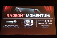
At its Computex presser, leading up to its 7 nm Radeon Vega series unveil, AMD touched upon the massive proliferation of the Vega graphics architecture, which is found not only in discrete GPUs, but also APUs, and semi-custom SoCs of the latest generation 4K-capable game consoles. One such slide that created quite some flutter reads that "Vega" shipments are over 10 times greater than those of the "previous generation."

Normally you'd assume the previous-generation of "Vega" to be "Polaris," since we're talking about the architecture, and not an implementation of it (eg: "Vega 10" or "Raven Ridge," etc.). AMD later, at its post event round-table, clarified that it was referring to "Fiji," or the chip that went into building the Radeon R9 Fury X, R9 Nano, etc., and comparing its sales with that of products based on the "Vega 10" silicon. Growth in shipments of "Vega" based graphics cards is triggered by the crypto-mining industry, and for all intents and purposes, AMD considers the "Vega 10" silicon to be a commercial success.
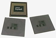
Samsung to Power Future High-Performance Computing and Connected Devices

Samsung Electronics, a world leader in advanced semiconductor technology solutions, today unveiled a series of new silicon innovations at the heart of future high-performance computing and connected devices. With comprehensive process technology roadmap updates down to 3-nanometer (nm) at the annual 'Samsung Foundry Forum (SFF) 2018 USA', Samsung Foundry is focused on providing customers with the tools necessary to design and manufacture powerful, yet energy-efficient system-on-chips (SoC) for a wide range of applications.

"The trend toward a smarter, connected world has the industry demanding more from silicon providers," said Charlie Bae, executive vice president and head of the Foundry Sales & Marketing Team at Samsung Electronics. "To meet that demand, Samsung Foundry is powering innovation at the silicon level that will ultimately give people access to data, analysis, and insight in new and previously unthought-of ways to make human lives better. It is imperative for us to accomplish the first-time silicon success for our customers' next-generation chip designs."

TSMC to Bring 3D Stacked Wafers to Complex Silicon Designs, Such as GPUs

TSMC is close to adapt 3D stacked silicon wafers to complex silicon designs, such as graphics processors, using its new proprietary Wafer-on-Wafer (WoW) Advanced Packaging technology, which will be introduced with its 7 nm+ and 5 nm nodes. 3D stacked silicon fabrication is currently only implemented on "less complex" silicon designs, such as NAND flash, which don't run anywhere near as hot as complex designs ASIC designs, such as GPUs or CPUs. In its current form, TSMC achieved 2-layer stacks, in which two silicon layers that are "mirror images" of each other (for perfect alignment), sandwich bonding layers, through which pins for the upper layer pass through.

The bonding of the two layers is where the bulk of TSMC's innovations and "secret sauces" lie. For 3D NAND flash, multiple pancaked dies are wired out through their edges. You don't need as many pins to talk to a NAND flash die, as say a GPU die. For complex dies, designers have to pass thousands of pins through the "bottom layer," the connecting substrate, and eventually to the "top layer." The bottom layer hence is bumped out on both ends, one side interfacing with the package substrate for both dies, and the top side serving as a sort of substrate for the top die. This innovation is what TSMC calls "thru-silicon-vias" or TSVs.

MSI Intros Cubi N 8 GL Series Mini-PCs with Intel "Gemini Lake" SoCs

MSI introduced the Cubi N 8 GL line of compact mini-PCs powered by Intel "Gemini Lake" Celeron and Pentium Silver SoCs. These include variants with Celeron J4005 and Pentium Silver J5005. Despite "Gemini Lake" chips featuring dual-channel memory support, the Cubi N 8 GL only features one DDR4 SO-DIMM slot, which supports up to 8 GB of DDR4-2400 memory. Storage options include either an M.2-2280 slot with both SATA 6 Gbps and PCIe 2.0 x2 wiring, or a 2.5-inch drive bay with SATA 6 Gbps. An interesting inclusion here is the Intel Dual Band Wireless-AC 9461 WLAN card, which gives you 802.11ac (up to 433 Mbps), but Bluetooth 5.0. Other connectivity includes four USB 3.0 ports, HDMI 2.0 and D-Sub display outputs, and gigabit Ethernet. The company didn't reveal pricing.

Intel Could Develop its own big.LITTLE x86 Adaptation

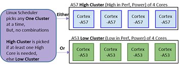
big.LITTLE is an innovation by ARM, which seeks to minimize power-draw on mobile devices. It is a sort of heterogeneous multi-core CPU design, in which a few "big" high-performance CPU cores work alongside a few extremely low-power "little" CPU cores. The idea here is that the low-power cores consume much lesser power at max load, than the high-performance cores at their minimum power-state, so the high-performance cores can be power-gated when the system doesn't need them (i.e. most of the time).

Intel finds itself with two distinct x86 implementations at any given time. It has low-power CPU micro-architectures such as "Silvermont," "Goldmont," and "Goldmont Plus," etc., implemented on low-power product lines such as the Pentium Silver series; and it has high-performance micro-architectures, such as "Haswell," "Skylake," and "Coffee Lake." The company wants to take a swing at its own heterogeneous multi-core CPU, according to tech stock analyst Ashraf Eassa, with the Motley Fool.

Apple to End the x86 Mac Era in 2020

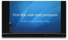
One of the biggest tech stories of the 2000s was Apple's transition from the PowerPC machine architecture to Intel x86, which brought the Mac closer to being the PC it so loathed. The transition wasn't smooth, as besides the operating system, practically every third-party software developer (eg: Adobe), had to rewrite their software for the new architecture, with new APIs, and new runtime environments. Apple could be bringing about a similar change before the turn of the decade.

Apple already builds its own application processors for iOS devices, and some of the newer chips such as the A11 Bionic and A10 Fusion have already reached the performance levels of entry-level x86 desktop processors. It's only a matter of time before Apple can build its own SoCs for Macs (that's not just iMac desktops, but also Mac Pro workstations, MacBook, MacBook Air, and MacBook Pro). That timeline is expected to be around 2020. Since these chips are based on the ARM machine architecture, they will mandate a major transformation of the entire software ecosystem Apple built over the past decade and a half. Intel shares dropped by as much as 9.2 at the first reports of this move.

Intel's "Bitcoin Mining Hardware Accelerator" Patent Filling Published

A filed patent by Intel has shed some light on the company's idea to somewhere, along the fuzzy lines of the future, introduce a Bitcoin mining hardware "accelerator" to the market. The application itself, for a "Bitcoin Mining Hardware Accelerator With Optimized Message Digest and Message Scheduler Datapath" was originally submitted in September 2016, so it's not exactly a novel idea. However, the fact that it has just now been published doesn't really mean there hasn't been work behind closed doors at Intel towards development of working silicon of this technology.

In the filing, it appears it's Intel's intent to create a chip that could augment the existing Bitcoin mining process by increasing energy efficiency. As they themselves put it, "Because the software and hardware utilized in Bitcoin mining uses brute force to repeatedly and endlessly perform SHA-256 functions, the process of Bitcoin mining can be very power-intensive and utilize large amounts of hardware space. The embodiments described herein optimize Bitcoin mining operations by reducing the space utilized and power consumed by Bitcoin mining hardware."

GIGABYTE Intros Brix S Powered by Pentium Silver J5005 SoC

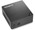
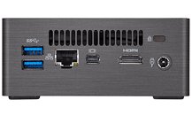
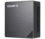
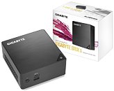
GIGABYTE today rolled out a variant of its Brix S mini-PC barebone powered by Pentium Silver J5005 SoC (model: GB-BLPD-5005). This chip packs a quad-core "Goldmont Plus" CPU, and faster UHD Graphics 605 iGPU than the one which Celeron J4005 comes with. You add your own DDR4 SO-DIMM memory (up to 8 GB of dual-channel memory over two slots); and storage. Storage options include an M.2-2280 slot with PCIe gen 2.0 x2 wiring, and a 2.5-inch drive bay with SATA 6 Gbps interface (up to 9.5 mm-thick drives supported).

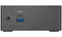
An included Intel Dual Band Wireless-AC 3168 card sitting in its own M.2 slot (other than the vacant M.2-2280 slot) provides dual-band 802.11 ac and Bluetooth 4.2. Wired networking is care of a Realtek RTL8111HS controller, putting out a GbE interface. The Realtek ALC255 HD audio codec puts out stereo audio with around 89 dBA SNR. USB connectivity includes four USB 3.0 ports (two on the rear panel, two up front, including a type-C port). Display outputs include one each of mini-DisplayPort 1.2a and HDMI 2.0a. Measuring 46.8 mm x 112.6 mm x 119.4 mm (HxWxD), it supports VESA mounting. The company didn't reveal pricing.

Xilinx Unveils Their Revolutionary Adaptive Compute Acceleration Platform

Xilinx, Inc., the leader in adaptive and intelligent computing, today announced a new breakthrough product category called adaptive compute acceleration platform (ACAP) that goes far beyond the capabilities of an FPGA. An ACAP is a highly integrated multi-core heterogeneous compute platform that can be changed at the hardware level to adapt to the needs of a wide range of applications and workloads. An ACAP's adaptability, which can be done dynamically during operation, delivers levels of performance and performance per-watt that is unmatched by CPUs or GPUs.

An ACAP is ideally suited to accelerate a broad set of applications in the emerging era of big data and artificial intelligence. These include: video transcoding, database, data compression, search, AI inference, genomics, machine vision, computational storage and network acceleration. Software and hardware developers will be able to design ACAP-based products for end point, edge and cloud applications. The first ACAP product family, codenamed "Everest," will be developed in TSMC 7nm process technology and will tape out later this year.

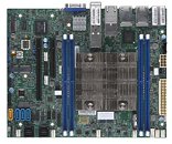
Supermicro Launches New Embedded Solutions Based on the Intel Xeon D-2100 SoC

Super Micro Computer, Inc. (NASDAQ: SMCI), a global leader in enterprise computing, storage, networking solutions and green computing technology, today announced several new additions to its edge computing and network appliance portfolio based on the new Intel Xeon D-2100 SoC (System-on-a-Chip) processor.

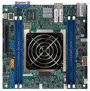
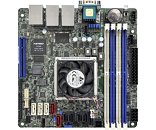
Leveraging its deep expertise in server technology, Supermicro is bringing customers some of the first Intel Xeon D-2100 System-on-a-Chip (SoC) processor-based solutions. The company's X11SDV series motherboards offer infrastructure optimization by combining the performance and advanced intelligence of Intel Xeon processors into a dense, lower-power system-on-a-chip. Supermicro is introducing a wide range of new systems to the market including compact embedded systems, rackmount embedded systems, as well as multi-node MicroCloud and SuperBlade systems.

Qualcomm to Build Snapdragon 5G SoCs on Samsung 7nm LPP EUV Process

Samsung Electronics, a world leader in advanced semiconductor technology, and Qualcomm Technologies, Inc., a subsidiary of Qualcomm Incorporated, today announced the intention to expand their decade-long foundry relationship into EUV (extreme ultra violet) lithography process technology, including the manufacture of future Qualcomm Snapdragon 5G mobile chipsets using Samsung's 7-nanometer (nm) LPP (Low Power Plus) EUV process technology.

Using 7LPP EUV process technology, Snapdragon 5G mobile chipsets will offer a smaller chip footprint, giving OEMs more usable space inside upcoming products to support larger batteries or slimmer designs. Process improvements, combined with a more advanced chip design, are expected to bring significant improvements in battery life.

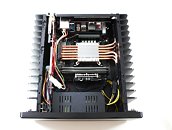
HDPlex H3 V2 Fanless Chassis Pictured

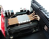
Here are some of the first pictures of HDPlex H3 V2 fan-less HTPC chassis. The H3 sits between the tiny H1 and deck-sized H5. It has the height of the H5 and the width of the H1. The case measures 270 mm x 264 mm x 93 mm (WxDxH), weighing in at 5.5 kg. Its main chamber can house mini-ITX motherboards, and a half-height add-on card that's no more than 1-slot thick. As with most fan-less cases, the chunky, ridged aluminium body of the H3 V2 doubles up as heatsink for the CPU/SoC, and can handle thermal loads of up to 80W. The CPU block uses eight 6 mm-thick copper heat pipes to transport heat to the body. The case also has room for up to four 7 mm-thick 2.5-inch drives. Available now, it is priced at USD $240.

Intel Launches Their Xeon D-2100 Series SoCs

Intel today introduced the new Intel Xeon D-2100 processor, a system-on-chip (SoC) processor architected to address the needs of edge applications and other data center or network applications constrained by space and power. The Intel Xeon D-2100 processor extends the record-breaking performance and innovation of the Intel Xeon Scalable platform from the heart of the data center to the network edge and web tier, where network operators and cloud service providers face the need to continuously grow performance and capacity without increasing power consumption.

"To seize 5G and new cloud and network opportunities, service providers need to optimize their data center and edge infrastructures to meet the growing demands of bandwidth-hungry end users and their smart and connected devices," said Sandra Rivera, senior vice president and general manager of the Network Platforms Group at Intel. "The Intel Xeon D-2100 processor allows service providers and enterprises to deliver the maximum amount of compute intelligence at the edge or web tier while expending the least power."

Samsung Enters Volume Production of a Killer Crypto-mining ASIC

One of the world's largest SoC, DRAM, and NAND flash makers, with its own semiconductor fabs, Samsung, is eyeing itself a large slice of the crypto-currency mining craze. The company reportedly entered volume production of a highly efficient crypto-currency mining ASIC, for an unnamed client from China. The client has placed a gargantuan order for crypto-coin mining ASICs contract-manufactured by Samsung, which appears to be targeted at Bitcoin, for now.

China's largest mining ASIC solutions providers, Bitman and Cannan, have similarly contracted TSMC to manufacture mining ASICs. An ASIC (from a mining context) is a single-chip solution that combines a CPU, a SIMD parallel-processing component tailored for mining, memory, and storage. It has infinitesimally smaller PCB, power, and thermal footprints compared to PCs with GPUs, and can be deployed in extremely large numbers for mining on an industrial-scale.

AMD 400-series Chipset Surfaces on PCI-SIG, PCIe 3.0 General Purpose Confirmed

AMD's second-generation Ryzen processors, which debut some time in Q1-2018, will be accompanied by the company's new 400-series motherboard chipset, even though they are expected to work with existing socket AM4 motherboards based on 300-series chipsets (with BIOS updates). The 400-series Promontory chipset surfaced on the PCIe Integrators List of PCI-SIG, the standards governing body of the PCI bus (which also oversees PCIe specifications development).

The listing seems to confirm that 400-series chipset will feature PCI-Express gen 3.0 general purpose lanes. These are downstream PCIe lanes put out by the chipset, to run the various external onboard controllers on the motherboard, and usually wired to the x1 and x4 PCIe slots. The current 300-series chipset only features up to 8 PCIe gen 2.0 general purpose lanes, and that was seen as a drawback. AMD Ryzen socket AM4 processors put out additional gen 3.0 lanes besides the 16 lanes allocated to PEG (one x16 or two x8, physically x16 slots); and 4 lanes serving as chipset bus. These additional gen 3.0 lanes typically drive a 32 Gb/s M.2 slot. With 400-series chipset bringing gen 3.0 general purpose lanes, one can expect newer socket AM4 motherboards with more than one 32 Gb/s M.2 slot (one from the SoC, another from the chipset).

Not Too Cool to Rule: One of NVIDIA's Most Coveted Products is a Ruler

"This is super cool;" "I've never seen anything like it;" "How do I get my hands on one?" Talk to NVIDIA recruiter Lisa Calderon and she'll tell you she has a secret weapon when it comes to getting tech's top talent talking to her. It's a foot long, one-and-a-half inches wide and covered with - to the uninitiated - strange gold markings. "Everyone asks the same thing," Calderon says. "'Can I have one?' And, of course, 'can I take another one for my 'friend'?'"

It's the NVIDIA ruler. And, as many NVIDIANs have learned, taking this modest slab of PCB board to the right place - and showing it to the right people - gets an immediate reaction. "Every electrical engineer that I've showed it to has instantly said 'I need one of these right now,'" says Josh, an NVIDIA ASIC architect, who has mailed bunches of them to contacts around the industry. Each time the ruler appears at NVIDIA's internal company store - which has sold 5,000 of these rulers so far - it sells out in minutes. Thousands more have been snatched up at industry conferences such as NIPS - the long-running deep-learning conference - where its appearance created a social media sensation. Employees at competitors will sidle up to our booth at industry events to trade bundles of their swag for it. It's never been made available to the public. But, if you're quick, you can find one on eBay for 10 times its modest employee-only price of $3.50 (when it's available). The only sure to way to get one: make friends with someone at NVIDIA.

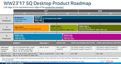
Latest Intel Roadmap Slide Leaked, Next Core X is "Cascade Lake-X"

The latest version of Intel's desktop client-platform roadmap has been leaked to the web, which reveals timelines and names of the company's upcoming product lines. To begin with, it states that Intel will upgrade its Core X high-end desktop (HEDT) product line only in Q4-2018. The new Core X HEDT processors will be based on the "Cascade Lake-X" silicon. This is the first appearance of the "Cascade Lake" micro-architecture. Intel is probably looking to differentiate its Ringbus-based multi-core processors (eg: "Coffee Lake," "Kaby Lake") from ones that use Mesh Interconnect (eg: "Skylake-X"), so people don't compare the single-threaded / less-parallized application performance between the two blindly.

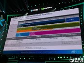
Next up, Intel is poised to launch its second wave of 6-core, 4-core, and 2-core "Coffee Lake" processors in Q1-2018, with no mentions of an 8-core mainstream-desktop processor joining the lineup any time in 2018. These processors will be accompanied by more 300-series chipsets, namely the H370 Express, B360 Express, and H310 Express. Q1-2018 also sees Intel update its low-power processor lineup, with the introduction of the new "Gemini Lake" silicon, with 4-core and 2-core SoCs under the Pentium Silver and Celeron brands.

Samsung Starts Mass Production of its 2nd Generation 10nm FinFET

Samsung Electronics, a world leader in advanced semiconductor technology, today announced that its Foundry Business has commenced mass production of System-on-Chip (SoC) products built on its second generation 10-nanometer (nm) FinFET process technology, 10LPP (Low Power Plus).

10LPP process technology allows up to 10-percent higher performance or 15-percent lower power consumption compared to its first generation 10nm process technology, 10LPE (Low Power Early). As this process is derived from the already proven 10LPE technology, it offers competitive advantages by greatly reducing turn-around time from development to mass production and by providing significantly higher initial manufacturing yield. SoCs designed with 10LPP process technology will be used in digital devices scheduled to launch early next year and are expected to become more widely available throughout the year.

Researchers Find Glaring Intel ME Security Flaws, Company Outs Detection Tool

Security researchers have found glaring security flaws with Intel Management Engine, the on-chip micro SoC that, besides governing the functionality of the processor, provides on-chip management and security features. These security flaws render "potentially millions" of PCs and notebooks, based on Intel processors, according to the researchers. Intel on Monday released a Detection Tool application that lets you identify vulnerabilities in the Management Engine of your Intel processor-powered PC, and suggests updates to Intel Management Engine drivers, or points to BIOS updates from your PC manufacturer.

Updates to Intel ME are specific to TXE 3.0 (trusted execution engine version 3.0), which is featured on processors based on "Skylake," "Kaby Lake," and "Coffee Lake" micro-architectures, across client- and enterprise market segments, and Atom processors released in the past three years. Intel chronicled this security flaw further under Security Advisory 86, and released the SA-00086 Detection Tool.

Intel NUC Based on Intel+Vega MCM Leaked

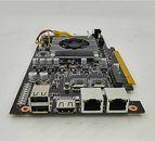
The first product based on Intel's ambitious "Kaby Lake-G" multi-chip module, which combines a quad-core "Kaby Lake-H" die with a graphics die based on AMD "Vega" architecture, will be a NUC (next unit of computing), and likely the spiritual successor to Intel's "Skull Canyon" NUC. The first picture of the motherboard of this NUC was leaked to the web, revealing a board that's only slightly smaller than the mini-ITX form-factor.

The board draws power from an external power brick, and appears to feature two distinct VRM areas for the CPU and GPU components of the "Kaby Lake-G" MCM SoC. The board feature two DDR4 SO-DIMM slots which are populated with dual-channel memory, and an M.2 NVMe slot, holding an SSD. There are two additional SATA 6 Gb/s ports, besides a plethora of other connectivity options.

Colorful Intros Unique C.J1900A-BTC PLUS V20 Mining Motherboard

Colorful today introduced the uniquely designed C.J1900A-BTC PLUS V20 motherboard for mining rigs. This odd-ball form-factor board is designed for makeshift racks, and removes the need for PCIe riser cables. The board itself is a large PCB with nine PCI-Express x16 slots with 1-slot spacing, of which eight can be used for installing your mining graphics cards (x1 wiring), while the slot on the middle (blue), isn't really a PCI-Express slot.

The blue slot has custom wiring for the business end of the motherboard, a riser card which houses the Celeron J1900 SoC, a DDR4 SO-DIMM slot, an mSATA 6 Gb/s slot for your SSD, and the board's main connectivity, which includes two USB 2.0 ports, two gigabit Ethernet interfaces, and an HDMI display output. If you have trouble finding an mSATA SSD in 2017, there's also a standard SATA 6 Gb/s port. The riser draws power from a 4-pin ATX input. The main PCB has eight 6-pin PCIe power inputs, which wire out to 6-pin PCIe outputs near each black slot. This is more of a cable-management feature, smaller (20 cm long) male-to-male 6-pin PCIe cables connect the outputs to the graphics cards.

Broadcom Looks to Buy Qualcomm for $100B, Creating a Silicon Monster

Broadcom, makers of networking equipment, is exploring a deal to acquire mobile technology giant Qualcomm in a USD $100 billion deal, which could be the largest ever acquisition value of a chip-maker. The resulting company could be the world's largest chipmaker, combining Broadcom's IP with networking PHYs and IoT infrastructure, and Qualcomm's SoCs powering IoT devices besides smartphones, tablets, and ultra-portable notebooks. Broadcom is looking to raise a cash+stock bid consisting of shares valued at $70/share. Besides networking infrastructure equipment, Broadcom made its fortunes on the back of Apple iPhone's success, as it supplies its networking chips.

ASRock Rack Intros C3758D4I-4L Mini-ITX Motherboard with Atom 8-core SoC

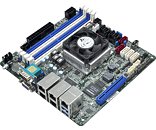
ASRock Rack, a new division of ASRock which deals with enterprise-grade motherboards, introduced the C3758D4I-4L, a mini-ITX motherboard based on the Atom C3758 "Denverton" SoC that embeds an 8-core CPU clocked at 2.20 GHz, 16 MB of cache, and a dual-channel DDR4 integrated memory controller supporting up to 256 GB of ECC memory, topped off with a 25W TDP. These specs lend Denverton quasi-enterprise credentials. The C3758D4I-4L can be used for low-cost rack-mount web-servers, or even high-end DIY NAS or home-server builds.

The C3758D4I-4L comes with a factory-fitted fan-heatsink cooling the pre-installed Atom C3758 BGA SoC. The board draws power from a combination of 24-pin ATX and 8-pin EPS power connectors (including a 4-pin connector for external 12V). The SoC is wired to four DDR4 DIMM slots, supporting up to 128 GB of dual-channel ECC memory; and a PCI-Express 3.0 x8 slot. Storage connectivity includes a staggering 13 SATA 6 Gbps ports, five on board, eight via two mini SAS connectors. An ASPeed AST2500 provides display, legacy I/O, and remote management. The board features a staggering five 1 GbE connections with teaming, PXE, and NCSI support. The company didn't reveal pricing.

Tesla Motors Develops Semi-custom AI Chip with AMD

Tesla Motors, which arguably brought electric vehicles to the luxury-mainstream, is investing big in self-driving cars. Despite its leader Elon Musk's fears and reservations on just how much one must allow artificial intelligence (AI) to develop, the company realized that a true self-driving car cannot be made without giving the car a degree of machine learning and AI, so it can learn its surroundings in real-time, and maneuver itself with some agility. To that extent, Tesla is designing its own AI processor. This SoC (system on chip) will be a semi-custom development, in collaboration with the reigning king of semi-custom chips, AMD.

AMD has with it a clear GPGPU performance advantage over NVIDIA, despite the latter's heavy investments in deep-learning. AMD is probably also banking on good pricing, greater freedom over the IP thanks to open standards, and a vast semi-custom track-record, having developed semi-custom chips with technology giants such as Sony and Microsoft. Musk confirmed that the first car in which you can simply get in, fall asleep, and wake up at your destination, will roll out within two years, hinting at a 2019 rollout. This would mean a bulk of the chip's development is done.

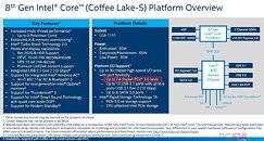
Intel "Coffee Lake" Platform Detailed - 24 PCIe Lanes from the Chipset

Intel seems to be addressing key platform limitations with its 8th generation Core "Coffee Lake" mainstream desktop platform. The first Core i7 and Core i5 "Coffee Lake" processors will launch later this year, alongside motherboards based on the Intel Z370 Express chipset. Leaked company slides detailing this chipset make an interesting revelation, that the chipset itself puts out 24 PCI-Express gen 3.0 lanes, that's not counting the 16 lanes the processor puts out for up to two PEG (PCI-Express Graphics) slots.

The PCI-Express lane budget of "Coffee Lake" platform is a huge step-up from the 8-12 general purpose lanes put out by previous-generation Intel chipsets, and will enable motherboard designers to cram their products with multiple M.2 and U.2 storage options, besides bandwidth-heavy onboard devices such as additional USB 3.1 and Thunderbolt controllers. The chipset itself integrates a multitude of bandwidth-hungry connectivity options. It integrates a 10-port USB 3.1 controller, from which six ports run at 10 Gbps, and four at 5 Gbps.
Return to Keyword Browsing
May 5th, 2024 11:35 EDT change timezone

New Forum Posts

Popular Reviews

Controversial News Posts