News Posts matching #SoC

Return to Keyword Browsing

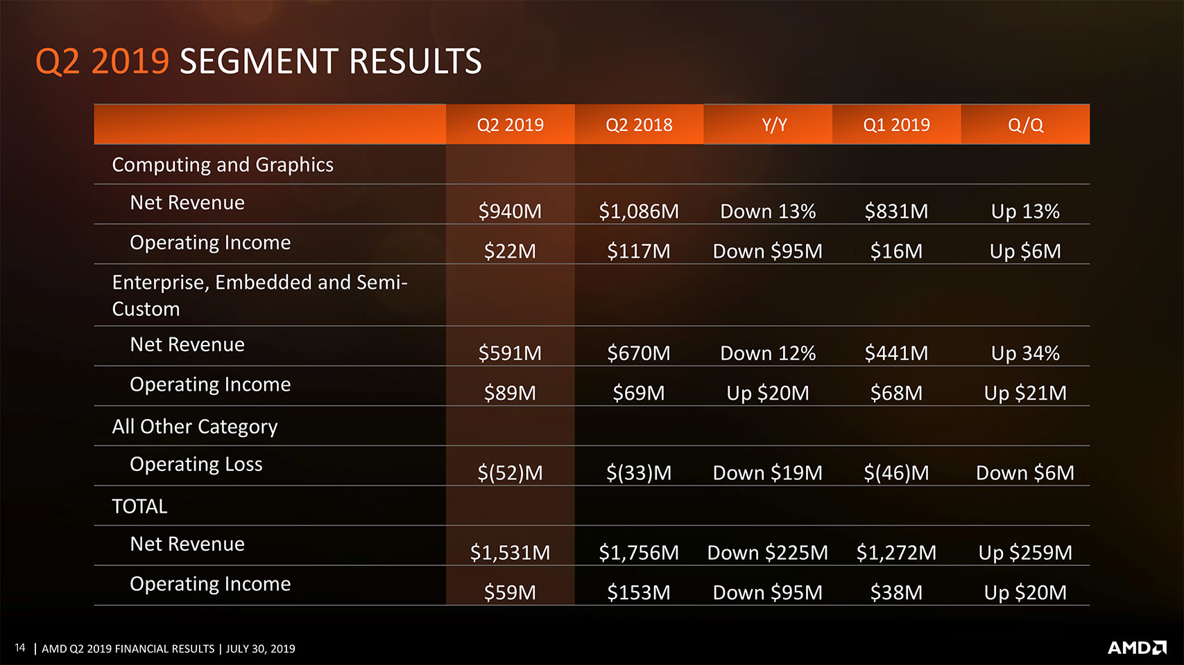
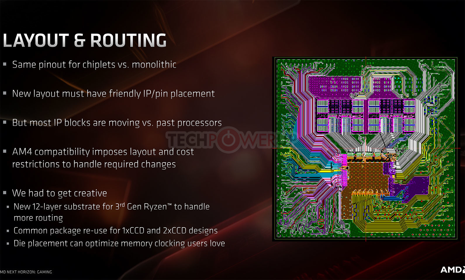
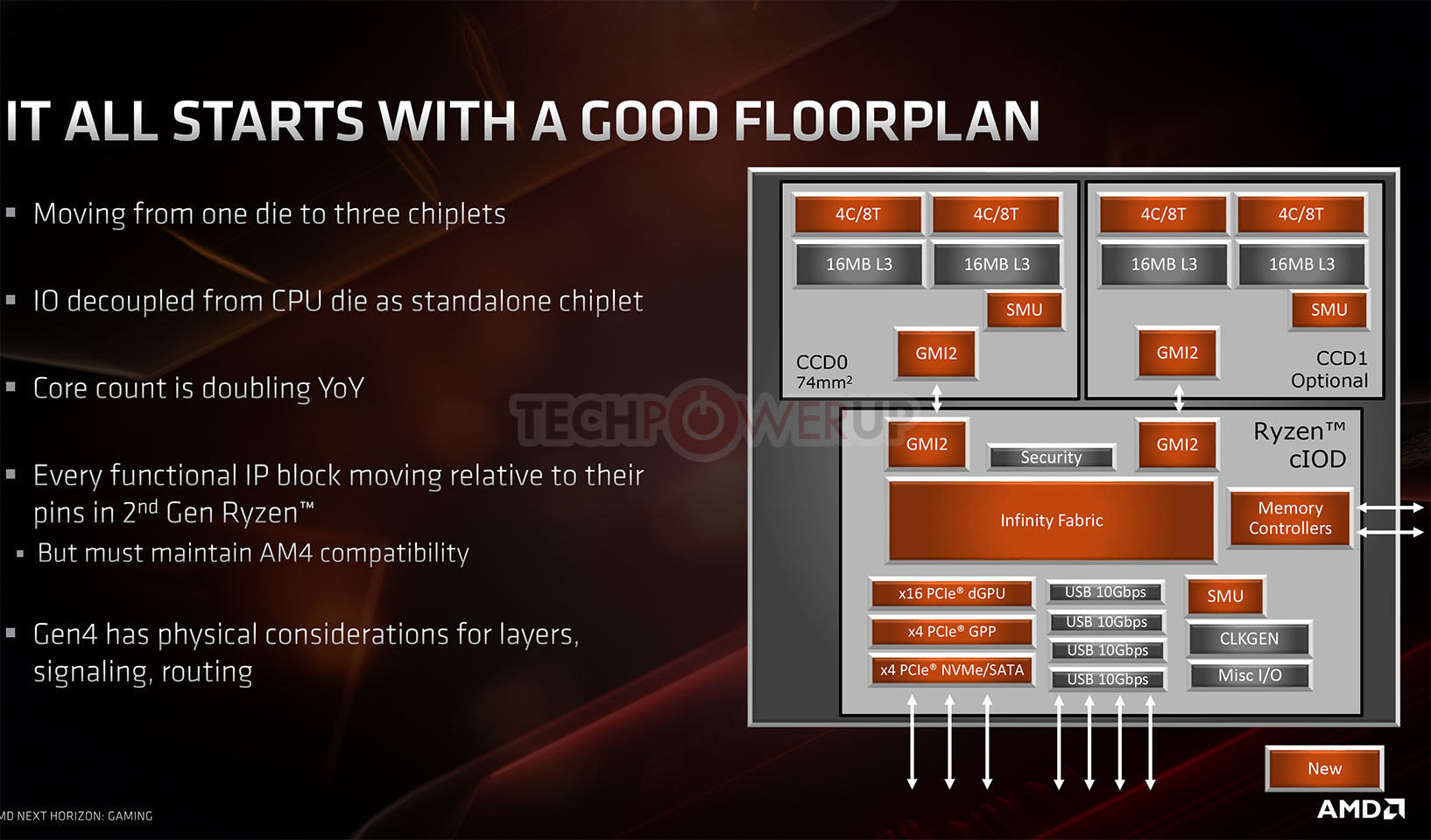
Intel Hires Former AMD GPU Silicon Executive

Intel's latest talent acquisition from rival AMD, as it builds a GPU product lineup, is Masooma Bhaiwala. "After 15+ amazing years at AMD, I have decided to take on a different opportunity... It was a truly fun ride, with an incredible team, during which we built some truly cool chips," she wrote in a LinkedIn post. According to her profile, Bhaiwala takes the role of Vice President, discrete GPU SoCs, and works under Intel's Graphics and Throughput Computing Hardware Engineering group headed by Raja Koduri.

Koduri's team has been a glassdoor for former AMD executives and tech-leads. While it has hired engineering talent such as Balaji Kanigicherla, Kalyan Thumaty and Joseph Facca; it has simultaneously lost client-graphics marketing talent, with the likes of Chris Hook, Heather Lennon, and Jon Carvill waltzing out of the company in less than a year of their association. Besides Koduri's Intel's most priced tech talent acquisition is Jim Keller, who is working on a future high-IPC CPU core design for the company. While working for AMD, Keller's "Zen" microarchitecture coupled with CEO Lisa Su's leadership have scripted one of the biggest turnarounds in Silicon Valley.

NVIDIA Introduces DRIVE AGX Orin Platform

NVIDIA today introduced NVIDIA DRIVE AGX Orin, a highly advanced software-defined platform for autonomous vehicles and robots. The platform is powered by a new system-on-a-chip (SoC) called Orin, which consists of 17 billion transistors and is the result of four years of R&D investment. The Orin SoC integrates NVIDIA's next-generation GPU architecture and Arm Hercules CPU cores, as well as new deep learning and computer vision accelerators that, in aggregate, deliver 200 trillion operations per second—nearly 7x the performance of NVIDIA's previous generation Xavier SoC.

Orin is designed to handle the large number of applications and deep neural networks that run simultaneously in autonomous vehicles and robots, while achieving systematic safety standards such as ISO 26262 ASIL-D. Built as a software-defined platform, DRIVE AGX Orin is developed to enable architecturally compatible platforms that scale from a Level 2 to full self-driving Level 5 vehicle, enabling OEMs to develop large-scale and complex families of software products. Since both Orin and Xavier are programmable through open CUDA and TensorRT APIs and libraries, developers can leverage their investments across multiple product generations.

AMD Announces Mini PC Initiative, Brings the Fight to Intel in Yet Another Product Segment

AMD is wading into even deeper waters across Intel's markets with the announcement of new Mini-PCs powered by the company's AMD Ryzen embedded V1000 and R1000 processors. Mini PCs, powered by AMD Ryzen Embedded V1000 and R1000 processors. Multiple partners such as ASRock Industrial, EEPD, OnLogic and Simply NUC have already designed their own takes on Mini-PCs (comparable to Intel's NUC, Next unit of Computing) as a way to give businesses a way to have a small form factor box for different computing needs. These aim to offer a high-performance CPU/GPU processor with expansive peripheral support, in-depth security features and a planned 10-year processor availability.

Until now, AMD's Ryzen Embedded product line had mostly scored one design win here and there, powering handheld consoles such as the Smach Z and such other low power, relatively high-performance environments. When AMD announced the R1000 SoC back in April, it already announced that partners would be bringing their own takes on the underlying silicon, and today is the announcement of that effort.

AWS Starts Designing 32-Core Arm Neoverse N1 CPU for Data Center

Amazon Web Services, a part of Amazon that is in charge of all things cloud, has announced plans to release 32 core CPU based on Arm Neoverse N1 microarchitecture that is designed to handle a diverse workload that today's cloud infrastructure needs. This new CPU should be the second iteration of AWS'es custom CPU based on the Arm architecture. First-generation AWS CPU was a processor called Graviton, which Amazon offered on-demand in the cloud.

The still-unnamed second-gen CPU will utilize a 7 nm manufacturing process if the Neoverce N1 core at its base is to be believed. Additionally, everything from the Neoverse line should translate to this next-gen CPU as well, meaning that there will be features like high frequency and high single-threaded performance, cache coherency, and interconnect fabric designed to connect special-purpose accelerators to the CPU complex. For reference, Arm's design of Neoverce N1 has a TDP of 105 W for the whole SoC and its packs 64 cores running at 3.1 GHz, delivering amazing power efficiency and high core count.

Imagination launches IMG A-Series Graphics Architecture: "The GPU of Everything"

Imagination Technologies announces the tenth generation of its PowerVR graphics architecture, the IMG A-Series. The fastest GPU IP ever released, IMG A-Series evolves the PowerVR GPU architecture to fulfil the graphics and compute needs of the full spectrum of next-generation devices. Designed to be "The GPU of Everything" IMG A-Series is the ultimate solution for multiple markets, from automotive, AIoT, and computing through to DTV/STB/OTT, mobile and server.

The IMG A-Series' multi-dimensional approach to performance scalability ranges from 1 pixel per clock (PPC) parts for the entry-level market right up to 2 TFLOP cores for performance devices, and beyond that to multi-core solutions for cloud applications. Dr. Ron Black, CEO, Imagination Technologies, says: "IMG A-Series is our most important GPU launch since we delivered the first mobile PowerVR GPU 15 years ago and the best GPU IP for mobile ever made. It offers the best performance over sustained time periods and at low power budgets across all markets. It really is the GPU of everything."

MediaTek Announces Dimensity & Dimensity 1000 5G SoC

MediaTek today unveiled Dimensity, MediaTek's family of powerful 5G system-on-chips (SoCs) offering an unrivaled combination of connectivity, multimedia, AI and imaging innovations for premium and flagship smartphones.

The MediaTek Dimensity 5G chipset family brings smart and fast together to power the world's most capable 5G devices. Dimensity represents a step toward a new era of mobility - the fifth dimension - to spur industry innovation and let consumers unlock the possibilities of 5G connectivity.

MSI Unveils Comet Lake Powered Cubi 5 10M Mini-PC

MSI updated its Cubi line of NUC-like mini-PCs with the new Cubi 5 10M, powered by 10th generation Core "Comet Lake" mobile processors. Measuring 124 mm x 124 mm X 53.7 mm (WxDxH), and weighing 550 g (excluding the power-brick), the Cubi 5 10M is powered by a Core i7 "Comet Lake-U" SoC (either i7-10510U quad-core or i7-10710U six-core), with its integrated UHD Graphics putting out pixels. Two DDR4 SO-DIMM slots let you drop in up to 64 GB of dual-channel memory, while your storage options are an M.2-2280 slot with both PCI-Express 3.0 x4 and SATA 6 Gbps wiring, and a 2.5-inch drive bay with SATA 6 Gbps. Connectivity includes USB 3.2 gen 1 type-C and type-A ports along the front panel, next to the audio jacks; additional type-A gen 1 ports at the rear; DisplayPort and HDMI making up the display outputs; a gigabit Ethernet interface driven by an Intel i219-V controller, and Intel AX201 WLAN card that provides 802.11ax and Bluetooth 5.0. The company didn't reveal pricing.

VIA CenTaur Develops a Multi-core x86 Processor for Enterprise with in-built AI Hardware

Tasting Intel's blood in the water with AMD's return to competitiveness, dormant x86 licensee VIA wants to take another swing at the market, this time with a multi-core processor targeted at enterprises and possibly workstations, developed by its subsidiary CenTaur. The company appears to want to cash in on the AI boom, and could develop turnkey facial-recognition CCTV solutions with the chip. CenTaur is ready with a working prototype. It features eight 64-bit x86 CPU cores, and an on-die "AI co-processor" named NCORE. A ringbus connects the eight CPU cores and the NCORE with the processor's other components. The processor features 16 MB of shared L3 cache, a quad-channel DDR4-3200 memory interface, and a 44-lane PCI-Express gen 3.0 root-complex, along with a fully integrated southbridge, making it an SoC. It also appears to be multi-socket capable, although VIA didn't detail the interconnect in use.

The NCORE is a PCI-mapped device to the software, which provides functions such as DNN building and training acceleration. From the looks of it, there's more to NCORE than simply a fixed-function hardware that multiplies matrices. Its developers state that the device accelerates AI at a rate of "20 trillion AI operations/sec with 20 terabytes/sec memory bandwidth." The CPU cores on the processor tick at 2.50 GHz, and while VIA hasn't made any IPC claims, it has mentioned support for the cutting-edge AVX-512 instruction-set, something even "Zen 2" lacks, which possibly indicates a powerful FPU. The silicon measures 195 mm², and has been built on 16 nm FinFET node at TSMC. VIA will demonstrate the unnamed processor and its testbed at ISC East 2019, held on November 20 and 21.

The full technology announcement slide-deck follows.

TechPowerUp and TerraMaster Present NAS Giveaway

TechPowerUp is partnering with TerraMaster to present the TerraMaster NAS Giveaway. Open for readers from the US and the EU, two randomly selected lucky winners stand a chance to get a TerraMaster F2-210 NAS. The F2-210 is the most powerful 2-bay NAS priced under USD $200, with a performance-optimized SoC for maximum throughput. It offers multiple layers of data-security over your network and the Internet. The TNAS interface is a powerful browser-based user-interface that lets you access your data over the local network and remotely, with a ton of security settings. Find out more about the F2-210 in its product page.

For more information and to participate, visit this page.

Intel "Frost Canyon" NUC Based on "Comet Lake" SoC Pictured

Here are some of the first pictures of Intel's new generation "Frost Canyon" NUC based on the company's 10th generation Core "Comet Lake-U" SoC. The top-spec variant, NUC10i7FN, is powered by a Core i7-10710U SoC, which packs a 6-core/12-thread CPU with 12 MB L3 cache, up to 4.70 GHz Turbo Boost, UHD Graphics clocked at 1.15 GHz, and 25 W cTDP (configurable TDP). The middle variant, NUC10i5FN, is powered by the 4-core/8-thread Core i5-10210U (up to 4.20 GHz CPU Turbo Boost, UHD Graphics with up to 1.00 GHz clocks, 8 MB L3 cache, and 25 W cTDP). At the entry level is the NUC10i3FN powered by the Core i3-10110U (2-core/4-thread CPU clocked up to 4.10 GHz, 4 MB L3 cache, UHD Graphics clocked up to 1.00 GHz, and 25 W cTDP).

Physically, these 10th generation NUCs look similar to their "Coffee Lake" powered predecessors codenamed "Bean Canyon," with the exception of just one each type-C and type-A USB 3.2 front panel ports. Other connectivity includes possible Wi-Fi 6 (802.11ax WLAN), 1 GbE, HDMI 2.0, Thunderbolt 3 with DP output on the top model, and an additional pair of 10 Gbps USB 3.2 ports. Intel is likely to launch "Frost Canyon" on December 12.

Samsung Shuts Down Its Custom CPU Design Group

According to the information obtained by Statesman, Samsung Electronics is shutting down its custom CPU design group within the company. Known for the designs of mobile SoCs like Exynos 9110, 9810 and 9820 just to name a few, it seems that there will be no more future developments of custom Exynos SoC for Samsung's mobile devices. Instead of designing its own cores, Samsung is now going to use ARM's reference A7x series of CPUs based on ARM v8 instruction set, with A76 or A77 being chosen as likely candidates for the high-performance workloads.

So far it is still unknown what will be inside new processors like the upcoming Exynos 9830 SoC, meant to power the next generation of mobile devices. But if things are like Samsung states, there should be reference ARM cores like A77 inside the new chip. Already announced chips like Exynos 990 are supposed to use a custom CPU core, while all future revisions of any new Exynos SoC will license a design IP from ARM. This decision is supposedly a by-product of being unable to compete with offers from Qualcomm, which offers faster "Snapdragon" SoCs. Samsung already uses the Snapdragon SoCs in its phones for the US and Chinese markets, while the rest of the world is getting an Exynos equivalent with the purchase of the same mobile device.

AMD Reports Third Quarter 2019 Financial Results

AMD (NASDAQ:AMD) today announced revenue for the third quarter of 2019 of $1.80 billion, operating income of $186 million, net income of $120 million and diluted earnings per share of $0.11. On a non-GAAP(*) basis, operating income was $240 million, net income was $219 million and diluted earnings per share was $0.18.

"Our first full quarter of 7 nm Ryzen, Radeon and EPYC processor sales drove our highest quarterly revenue since 2005, our highest quarterly gross margin since 2012 and a significant increase in net income year-over-year," said Dr. Lisa Su, AMD president and CEO. "I am extremely pleased with our progress as we have the strongest product portfolio in our history, significant customer momentum and a leadership product roadmap for 2020 and beyond."

GLOBALFOUNDRIES Introduces 12LP+ FinFET Solution for Cloud and Edge AI Applications

GLOBALFOUNDRIES (GF), the world's leading specialty foundry, announced today at its Global Technology Conference the availability of 12LP+, an innovative new solution for AI training and inference applications. 12LP+ offers chip designers a best-in-class combination of performance, power and area, along with a set of key new features, a mature design and production ecosystem, cost-efficient development and fast time-to-market for high-growth cloud and edge AI applications.

Derived from GF's existing 12nm Leading Performance (12LP) platform, GF's new 12LP+ provides either a 20% increase in performance or a 40% reduction in power requirements over the base 12LP platform, plus a 15% improvement in logic area scaling. A key feature is a high-speed, low-power 0.5 V SRAM bit cell that supports the fast, power-efficient shuttling of data between processors and memory, an important requirement for AI applications in the computing and wired infrastructure markets.

Intel Ships First 10nm Agilex FPGAs

Intel today announced that it has begun shipments of the first Intel Agilex field programmable gate arrays (FPGAs) to early access program customers. Participants in the early access program include Colorado Engineering Inc., Mantaro Networks, Microsoft and Silicom. These customers are using Agilex FPGAs to develop advanced solutions for networking, 5G and accelerated data analytics.

"The Intel Agilex FPGA product family leverages the breadth of Intel innovation and technology leadership, including architecture, packaging, process technology, developer tools and a fast path to power reduction with eASIC technology. These unmatched assets enable new levels of heterogeneous computing, system integration and processor connectivity and will be the first 10nm FPGA to provide cache-coherent and low latency connectivity to Intel Xeon processors with the upcoming Compute Express Link," said Dan McNamara, Intel senior vice president and general manager of the Networking and Custom Logic Group.

Xilinx Announces Virtex UltraScale+, the World's Largest FPGA

Xilinx, Inc., the leader in adaptive and intelligent computing, today announced the expansion of its 16 nanometer (nm) Virtex UltraScale+ family to now include the world's largest FPGA — the Virtex UltraScale+ VU19P. With 35 billion transistors, the VU19P provides the highest logic density and I/O count on a single device ever built, enabling emulation and prototyping of tomorrow's most advanced ASIC and SoC technologies, as well as test, measurement, compute, networking, aerospace and defense-related applications.

The VU19P sets a new standard in FPGAs, featuring 9 million system logic cells, up to 1.5 terabits per-second of DDR4 memory bandwidth and up to 4.5 terabits per-second of transceiver bandwidth, and over 2,000 user I/Os. It enables the prototyping and emulation of today's most complex SoCs as well as the development of emerging, complex algorithms such as those used for artificial intelligence, machine learning, video processing and sensor fusion. The VU19P is 1.6X larger than its predecessor and what was previously the industry's largest FPGA — the 20 nm Virtex UltraScale 440 FPGA.

Intel Launches First 10th Gen Core Processors: Redefining the Next Era of Laptop Experiences

Today, Intel officially launched 11 new, highly integrated 10th Gen Intel Core processors designed for remarkably sleek 2 in 1s and laptops. The processors bring high-performance artificial intelligence (AI) to the PC at scale, feature new Intel Iris Plus graphics for stunning entertainment and enable the best connectivity with Intel Wi-Fi 6 (Gig+) and Thunderbolt 3. Systems are expected from PC manufacturers for the holiday season.

"These 10th Gen Intel Core processors shift the paradigm for what it means to deliver leadership in mobile PC platforms. With broad-scale AI for the first time on PCs, an all-new graphics architecture, best-in-class Wi-Fi 6 (Gig+) and Thunderbolt 3 - all integrated onto the SoC, thanks to Intel's 10nm process technology and architecture design - we're opening the door to an entirely new range of experiences and innovations for the laptop."
-Chris Walker, Intel corporate vice president and general manager of Mobility Client Platforms in the Client Computing Group

AMD Reports Second Quarter 2019 Financial Results

AMD (NASDAQ:AMD) today announced revenue for the second quarter of 2019 of $1.53 billion, operating income of $59 million, net income of $35 million and diluted earnings per share of $0.03. On a non-GAAP basis, operating income was $111 million, net income was $92 million and diluted earnings per share was $0.08.

"I am pleased with our financial performance and execution in the quarter as we ramped production of three leadership 7nm product families," said Dr. Lisa Su, AMD president and CEO. "We have reached a significant inflection point for the company as our new Ryzen, Radeon and EPYC processors form the most competitive product portfolio in our history and are well positioned to drive significant growth in the second half of the year."

BIOSTAR Formally Enables PCIe Gen 4 on its AMD 400-series Motherboards

BIOSTAR formally (officially) enabled PCI-Express gen 4.0 support for four of its socket AM4 motherboard models based on the AMD X470 and B450 chipsets, through BIOS updates. The updated BIOS lets you use PCI-Express gen 4.0 graphics cards on the topmost PCI-Express x16 slot, and the M.2 NVMe slot that's directly wired to the AM4 SoC. The expansion slots that are wired to the chipset are still restricted to PCIe gen 2.0. You will need a 3rd generation Ryzen "Matisse" processor for PCI-Express gen 4.0. Among the motherboards that receive PCIe gen 4.0 support through BIOS updates are the AB45C-M4S (B450MH), the AB35G-M4S (B45M2), the AX47A-A4T (X470GT8), and the AX47A-I4S (X470GTN). The links lead to the BIOS image files on BIOSTAR website, which you use at your own risk.

ASUS Begins Enabling Limited PCIe Gen 4.0 on AMD 400-series Chipset Motherboards

ASUS believes that PCI-Express gen 4.0 support on older socket AM4 motherboards based on the AMD 400-series chipset is technically possible, even if discouraged by AMD. The company's latest series of motherboard BIOS updates that expose PCIe Gen 4 toggle in the PCIe settings, does in fact enable PCIe gen 4.0 to all devices that are directly wired to the SoC. These would be the PCI-Express x16 slots meant for graphics, and one of the M.2 slots that has PCIe x4 wiring to the SoC. Below is a list of motherboards scored by Chinese tech publication MyDrivers, which details the extent of PCIe gen 4.0 support across a number of ASUS motherboards based on the X470 and B450 chipsets.

AMD apparently did not explicitly block PCIe gen 4.0 for older chipsets. It merely suggested to motherboard manufacturers not to enable it, since the newer AMD 500-series motherboards are built to new PCB specifications that ensure PCIe gen 4.0 signal-integrity and stability. ASUS wants to leave it to users to decide if they want gen 4.0. If their machines are unstable, they can choose to limit PCIe version to gen 3.0 in their BIOS settings. Among other things, AMD's specifications for 500-series chipset motherboards prescribe PCBs with more than 4 layers, for optimal PCIe and memory wiring. Many of the motherboards on ASUS' list, such as the TUF B450 Pro Gaming, use simple 4-layer PCBs.

NVIDIA Brings CUDA to ARM, Enabling New Path to Exascale Supercomputing

NVIDIA today announced its support for Arm CPUs, providing the high performance computing industry a new path to build extremely energy-efficient, AI-enabled exascale supercomputers. NVIDIA is making available to the Arm ecosystem its full stack of AI and HPC software - which accelerates more than 600 HPC applications and all AI frameworks - by year's end. The stack includes all NVIDIA CUDA-X AI and HPC libraries, GPU-accelerated AI frameworks and software development tools such as PGI compilers with OpenACC support and profilers. Once stack optimization is complete, NVIDIA will accelerate all major CPU architectures, including x86, POWER and Arm.

"Supercomputers are the essential instruments of scientific discovery, and achieving exascale supercomputing will dramatically expand the frontier of human knowledge," said Jensen Huang, founder and CEO of NVIDIA. "As traditional compute scaling ends, power will limit all supercomputers. The combination of NVIDIA's CUDA-accelerated computing and Arm's energy-efficient CPU architecture will give the HPC community a boost to exascale."

AMD B550 and A520 Lack PCIe Gen 4 Capabilities?

Last Friday, we reported ASMedia working on new-generation socket AM4 motherboard chipsets that succeed the AMD B450 and A320, which could hopefully offer significantly cheaper alternatives to boards based on the feature-rich AMD X570 chipset. The DigiTimes story we cited was updated to clarify that the chipset only supports PCI-Express gen 3.0, and not the newer PCI-Express gen 4.0. There are two distinct ways of interpreting this information.

One, that motherboards based on B550 and A520 completely lack PCIe gen 4.0, including the main PCI-Express x16 (PEG) slot and the M.2 slot wired to the AM4 SoC; and two, that only the downstream PCIe lanes and the chipset bus are PCIe gen 3.0, while the main PEG slot and M.2 slot from the SoC remain gen 4. We lean toward the latter interpretation being more plausible, that AMD B550 and A520 motherboards will at least feature one PCI-Express 4.0 x16 slot, and one M.2 slot that has PCI-Express 4.0 x4 wiring from the AM4 SoC; while the ASMedia chipset is connected to the SoC over PCI-Express 3.0 x4, and downstream PCIe lanes put out by the chipset are gen 3.0, too. These ASMedia-sourced AMD 500-series chipset motherboards could also implement the latest PCB, CPU VRM, and memory wiring specifications released by AMD that enable CPU and memory overclocking levels unattainable on motherboards based on older chipsets.

AMD Ryzen 3000 "Matisse" I/O Controller Die 12nm, Not 14nm

AMD Ryzen 3000 "Matisse" processors are multi-chip modules of two kinds of dies - one or two 7 nm 8-core "Zen 2" CPU chiplets, and an I/O controller die that packs the processor's dual-channel DDR4 memory controller, PCI-Express gen 4.0 root-complex, and an integrated southbridge that puts out some SoC I/O, such as two SATA 6 Gbps ports, four USB 3.1 Gen 2 ports, LPCIO (ISA), and SPI (for the UEFI BIOS ROM chip). It was earlier reported that while the Zen 2 CPU core chiplets are built on 7 nm process, the I/O controller is 14 nm. We have confirmation now that the I/O controller die is built on the more advanced 12 nm process, likely GlobalFoundries 12LP. This is the same process on which AMD builds its "Pinnacle Ridge" and "Polaris 30" chips. The 7 nm "Zen 2" CPU chiplets are made at TSMC.

AMD also provided a fascinating technical insight to the making of the "Matisse" MCM, particularly getting three highly complex dies under the IHS of a mainstream-desktop processor package, and perfectly aligning the three for pin-compatibility with older generations of Ryzen AM4 processors that use monolithic dies, such as "Pinnacle Ridge" and "Raven Ridge." AMD innovated new copper-pillar 50µ bumps for the 8-core CPU chiplets, while leaving the I/O controller die with normal 75µ solder bumps. Unlike with its GPUs that need high-density wiring between the GPU die and HBM stacks, AMD could make do without a silicon interposer or TSVs (through-silicon-vias) to connect the three dies on "Matisse." The fiberglass substrate is now "fattened" up to 12 layers, to facilitate the inter-die wiring, as well as making sure every connection reaches the correct pin on the µPGA.

Xbox "Project Scarlett" to be 8K and Ray-tracing Ready, AMD-powered, Coming 2020

Microsoft at its E3 2019 keynote dropped a huge teaser of its next-generation gaming console development, codenamed "Project Scarlett." The console is expected to pack some serious hardware that powers gaming at 8K resolution (that's four times 4K, sixteen times Full HD). That's not all, it will also feature real-time ray-tracing. Microsoft's performance target for the console is to be 4 times higher than that of the Xbox One X. The company is also giving the console its first major storage sub-system performance update in years.

At its heart is a new 7 nm semi-custom SoC by AMD and a high degree of customization by Microsoft. This chip features CPU cores based on the "Zen 2" microarchitecture, which provide a massive leap in CPU performance over the current Scorpio Engine SoC that uses low-power "Jaguar Enhanced" cores. At the helm of graphics is a new iGPU based on the RDNA architecture that powers AMD's upcoming Radeon RX 5000 "Navi" graphics cards. It's interesting here to note that Microsoft talks about real-time ray-tracing while we're yet to see evidence of any specialized ray-tracing hardware on "Navi." In its teaser, however, Microsoft stressed on the ray-tracing feature being "hardware-accelerated."

ECS Shows Off LIVA and SFF Desktops Powered by Ice Lake, and Possibly Picasso

ECS at its Computex 2019 booth showed off its next generation of LIVA branded mini PCs and a new AMD platform SFF desktop. We begin with the retro-looking SF110-A320, an SFF desktop measuring 205 mm x 176 mm x 33 mm (WxDxH), with an AM4 socket, and the ability to power 35W TDP APUs. Its mainboard is driven by an AMD A320 chipset. We know that the A320 supports 12 nm Ryzen 3000-series "Picasso" APUs. It's quite possible that these desktops could ship with them, particularly their low-TDP variants. The iGPU of these chips are wired out to two DisplayPorts, an HDMI, and a D-sub (VGA) output. You drop in your own DDR4 SO-DIMM modules, an M.2-2280 SSD, or 2.5-inch SATA drive. Networking options include 802.11ac WLAN, Bluetooth 4.2, and 1 GbE wired networking. ECS includes a 90W power-brick.

The company also showed off its latest LIVA Z3 Plus series mini PCs that appear to be ready for 10th generation Core "Ice Lake-U" SoCs, although the company won't mention it. There are two physical variants of the Z3 Plus, a shorter one that lacks a 2.5-inch drive bay, making you rely entirely on an M.2-2280 slot for internal storage (PCIe + SATA); and a taller variant with an additional 2.5-inch drive bay with SATA 6 Gbps. The shorter variant measures 117 mm x 128 mm x 37 mm (WxDxH), and the taller one about 47 mm in height. Both variants ship with 120W power bricks, take in two DDR4 SO-DIMM modules, one M.2-2280 SSD, and put out connectivity that includes HDMI and mDP display outputs, dual 1 GbE wired + 802.11ac + Bluetooth 4.2 networking, and four USB 3.1 gen 2 ports, from which one is a type-C.

AMD Announces 3rd Generation Ryzen Desktop Processors

AMD CEO Dr. Lisa Su at her 2019 Computex keynote address announced the 3rd generation Ryzen desktop processor family, which leverages the company's Zen 2 microarchitecture, and are built on the 7 nm silicon fabrication process at TSMC. Designed for the AM4 CPU socket, with backwards compatibility for older AMD 300-series and 400-series chipset motherboards, these processors are multi-chip modules of up to two 8-core "Zen 2" CPU chiplets, and a 14 nm I/O controller die that packs the dual-channel DDR4 memory controller and PCI-Express gen 4.0 root complex, along with some SoC connectivity. AMD claims an IPC increase of 15 percent over Zen 1, and higher clock speeds leveraging 7 nm, which add up to significantly higher performance over the current generation. AMD bolstered the core's FPU (floating-point unit), and doubled the cache sizes.

AMD unveiled three high-end SKUs for now, the $329 Ryzen 7 3700X, the $399 Ryzen 7 3800X, and the $499 Ryzen 9 3900X. The 3700X and 3800X are 8-core/16-thread parts with a single CPU chiplet. The 3700X is clocked at 3.60 GHz with 4.40 GHz maximum boost frequency, just 65 Watts TDP and will be beat Intel's Core i7-9700K both at gaming and productivity. The 3800X tops that with 3.90 GHz nominal, 4.50 GHz boost, 105W TDP, and beat the Core i9-9900K at gaming and productivity. AMD went a step further at launched the new Ryzen 9 brand with the 3900X, which is a 12-core/24-thread processor clocked at 3.80 GHz, which 4.60 boost, 72 MB of total cache, 105W TDP, and performance that not only beats the i9-9900K, but also the i9-9920X 12-core/24-thread HEDT processor despite two fewer memory channels. AMD focused on gaming performance with Zen 2, with wider FPU, improved branch prediction, and several micro-architectural improvements contributing to a per-core performance that's higher than Intel's. The processors go on sale on 7/7/2019.
Return to Keyword Browsing
May 9th, 2024 01:25 EDT change timezone

New Forum Posts

Popular Reviews

Controversial News Posts