 340
340
AMD Ryzen 7 7800X3D Review - The Best Gaming CPU
Socket AM5 Platform »3D Vertical Cache Technology
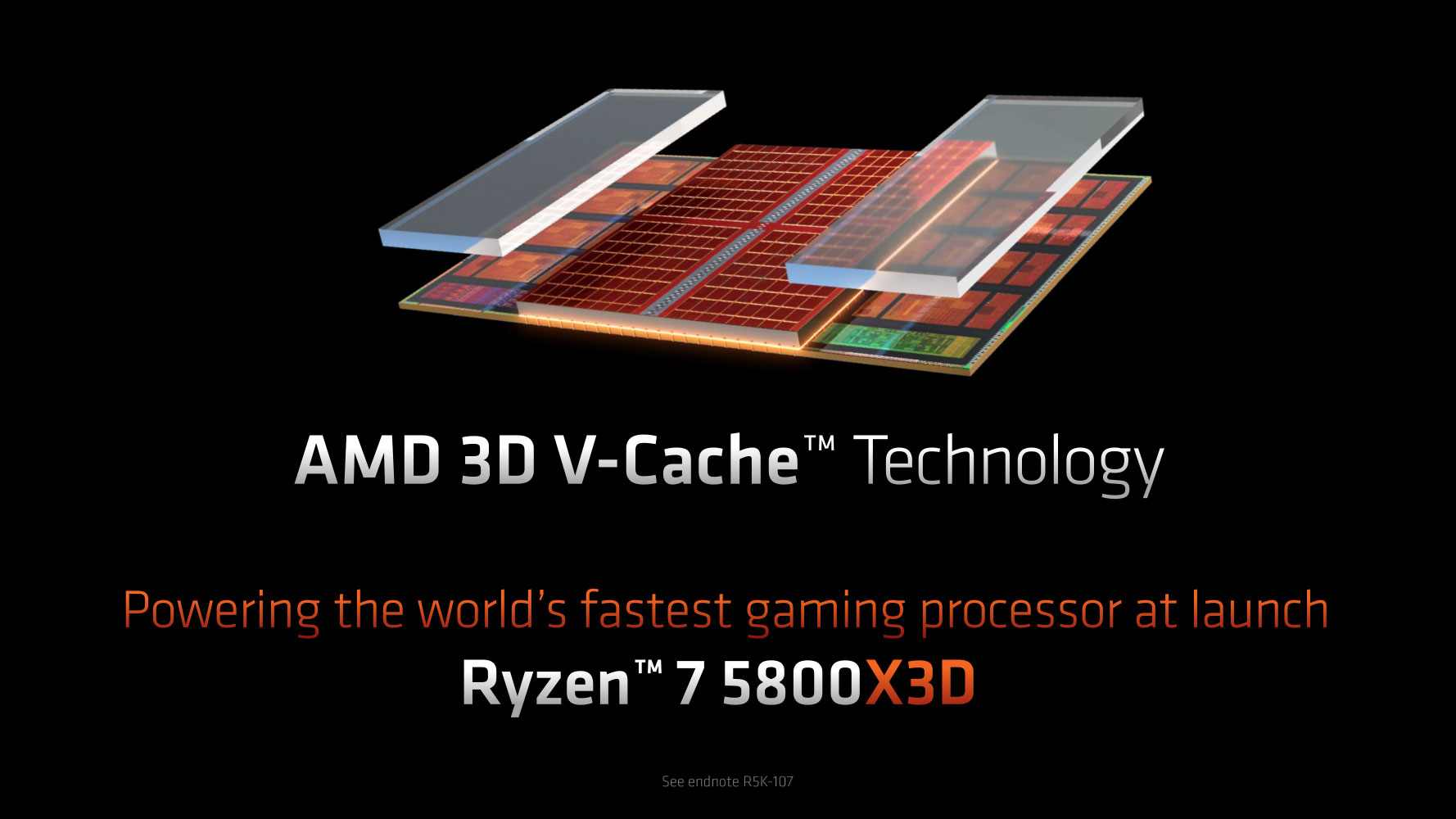
3D Vertical Cache is an additional 64 MB cache on a dedicated piece of silicon, which is placed on top of the region of the "Zen 4" CCD that has the 32 MB on-die L3 cache, and connected via TSVs (through-silicon vias). This cache operates at the same speed as the on-die L3 cache, and is hence designed to be contiguous to it. Software and OS see just a single 96 MB chunk of L3 cache for the CCD—it's not split into two separate chunks. Large, fast cache memory close to the logic, has been found to have a significant positive impact on gaming performance.
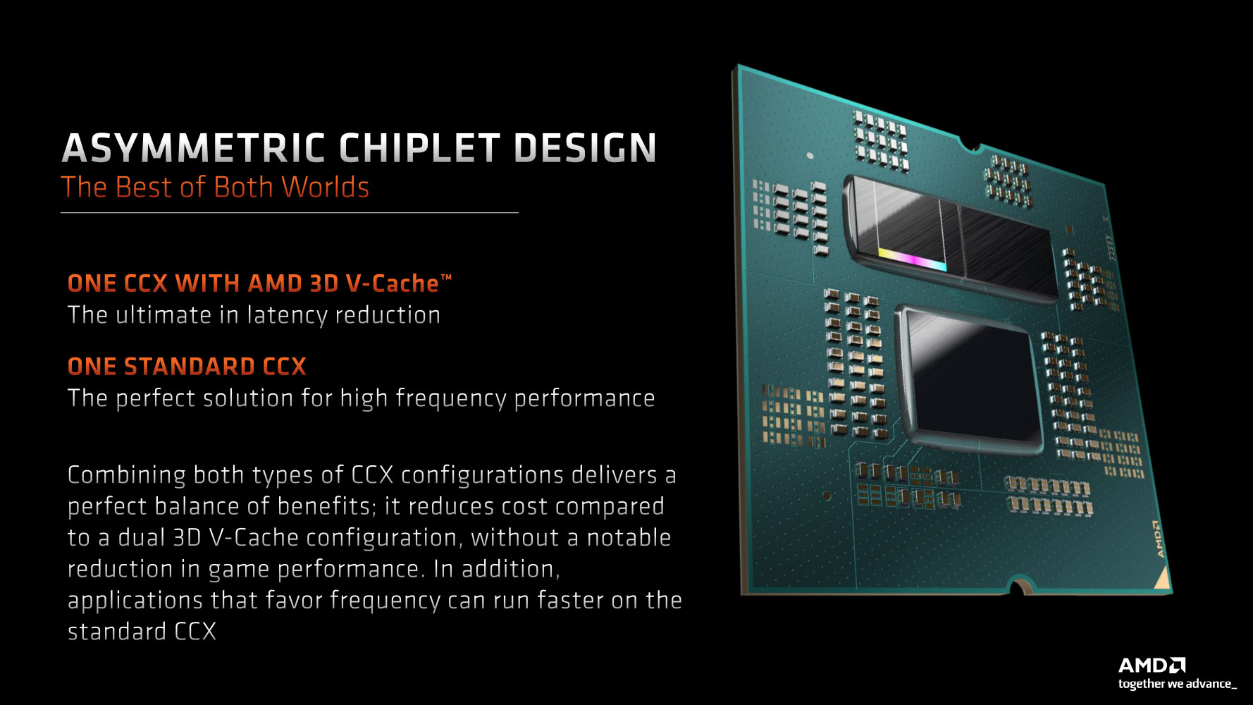
At a physical level, the 3D Vertical Cache is a 64 MB SRAM placed on a silicon die built on the 6 nm process; AMD refers to this die as simply the L3 Cache Die (L3D), which is stacked on top of the CPU Complex Die (CCD). Since this adds to the vertical thickness of the CCD towards its center, the edges of the CCD that have the all-important CPU cores, are layered with a highly conductive structural silicon that levels out the die. Soldered TIM then bonds the CCD with the processor's copper integrated heatspreader (IHS). While the 7950X3D and 7900X3D are dual-CCD (dual-chiplet) processors that have to deal with getting the OS scheduling just right for games to benefit from 3DV cache, the 7800X3D in this review is a single-CCD processor, and has no such issues.
The Zen 4 Platform

AMD Zen has been one of the most remarkable turnarounds for a company in the semiconductor industry, and has had a profound impact on the consumer, as it influenced Intel's CPU core-counts. With each new generation of Zen, AMD delivered IPC and overall performance improvements, and Zen 4 stands out as it not only aims to improve performance, but also introduce a brand-new platform after five years of Socket AM4. As a parting gift, AMD enabled official Zen 3 support on even the oldest 300-series chipset, going to show just how consumer-friendly AM4 was, something the company hopes to repeat with AM5. The new AM5 socket was needed as the company enables the latest I/O, including DDR5 memory and PCI-Express Gen 5, besides power-delivery improvements. The socket can now deliver up to 230 W of power, which gives AMD room to increase CPU core-counts in the future. AM5 is a land-grid array, just like Intel desktop sockets, but the company retained CPU cooler compatibility with AM4.
Zen 4 Chip Configuration
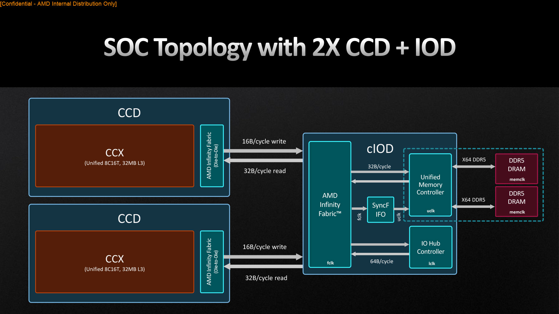
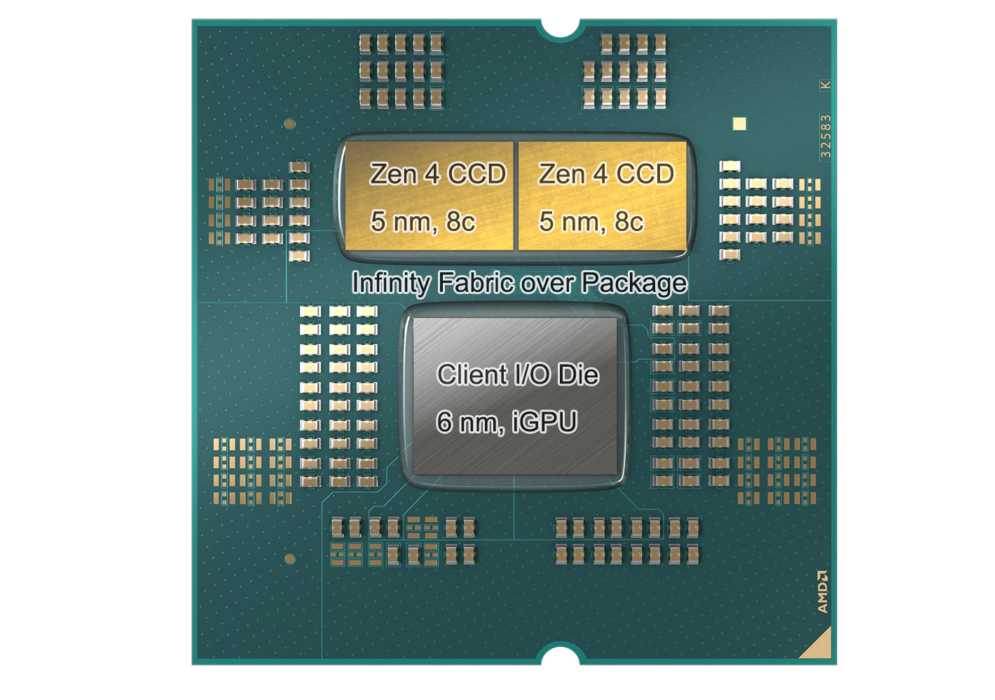
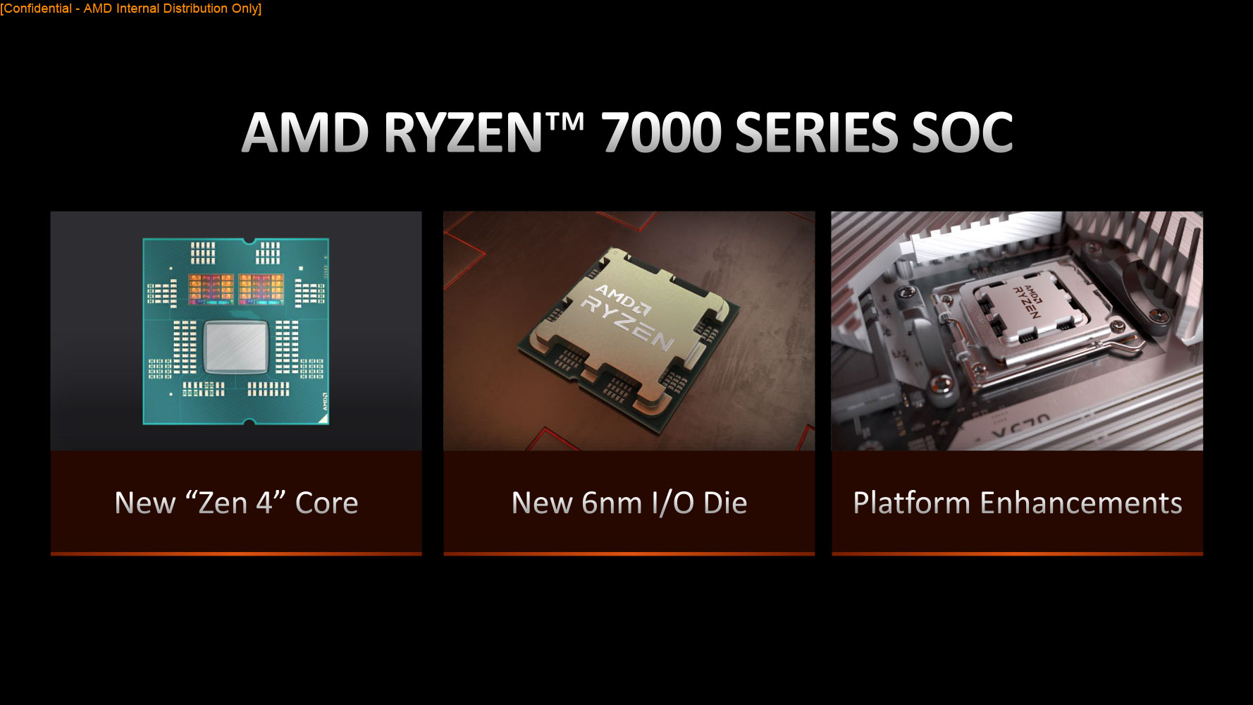
The Ryzen 7000 series desktop processor, codenamed "Raphael," is a multi-chip module, just like the Ryzen 5000 "Vermeer" and Ryzen 3000 "Matisse." The CPU cores are located in specialized dies called CCDs (CPU complex dies), while the platform I/O control is located in a separate die called cIOD (client I/O die). The CCDs were fabricated on the latest TSMC 5 nm EUV (N5) node, while the cIOD are done so on TSMC 6 nm (N6) nodes. The idea here is that the parts that benefit the most from the switch to the latest foundry process—the CPU cores—are built on this node; while everything else that can do with a slightly older node, uses that instead. This way AMD can make the most of its 5 nm foundry allocation with TSMC. The MCM contains a cIOD, and two 8-core CCDs in case of the Ryzen 9 7950X and 7900X; or one 8-core CCD in case of the Ryzen 7 7700X and Ryzen 5 7600X. Infinity Fabric interconnect handles communications not just within these dies, but also between them. The transition to fast DDR5 memory and PCIe Gen 5 means that AMD now can push instructions and data around faster. It did so with microarchitectural improvements to the "Zen 4" core itself, while also increasing the Infinity Fabric bandwidth between the cores.
The Zen 4 CPU Core
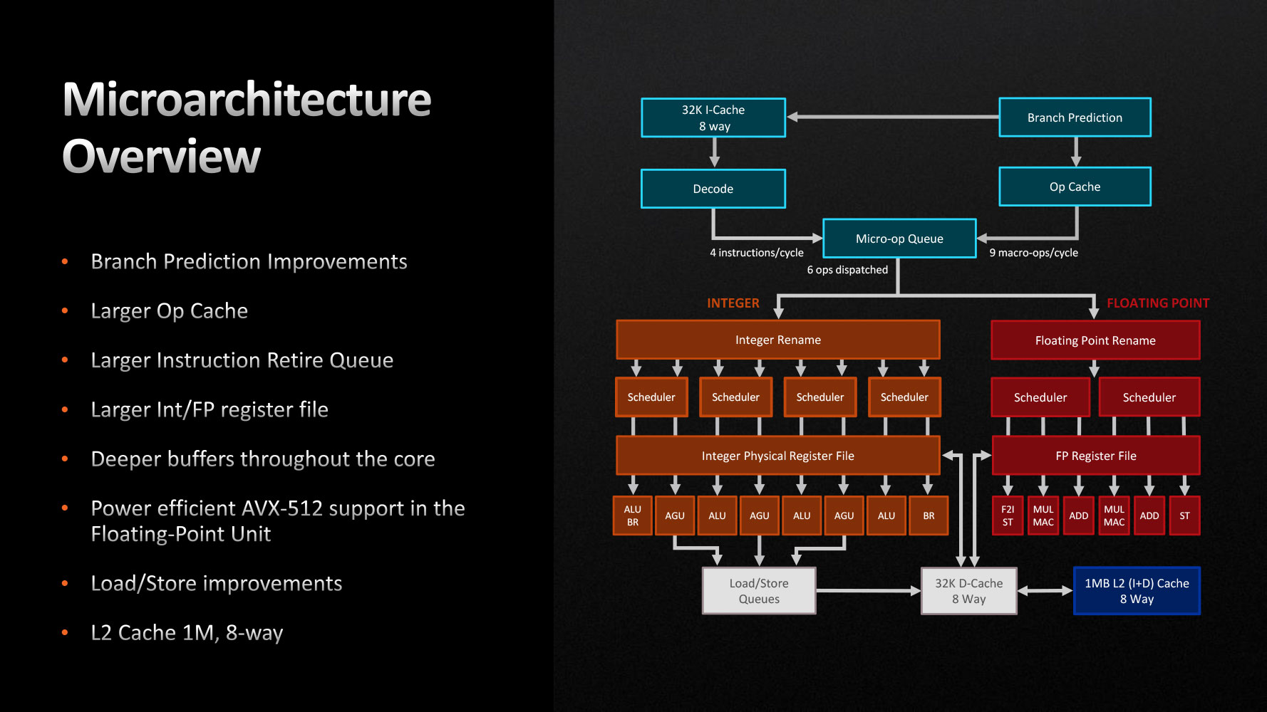
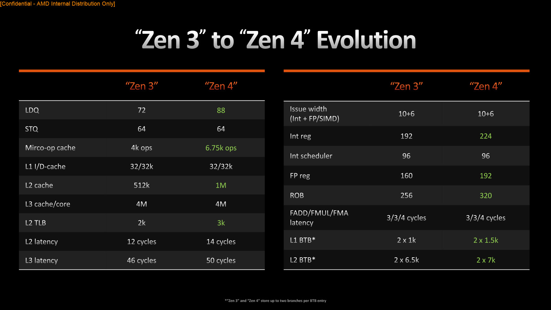
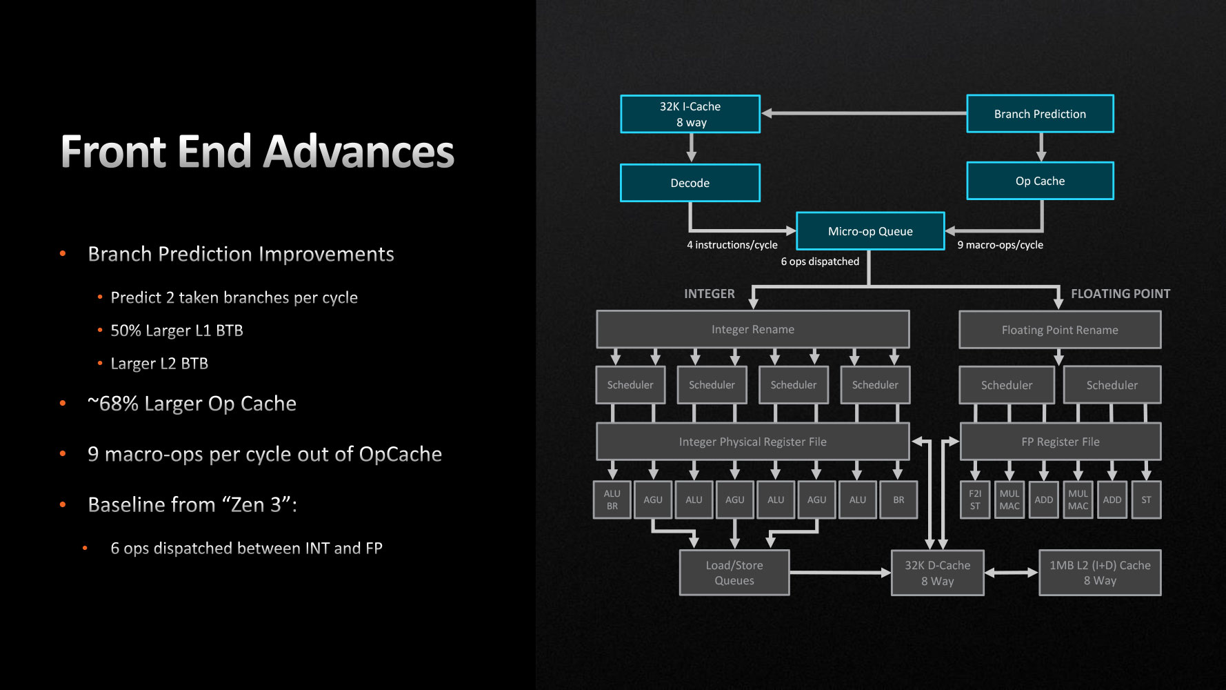
All cores in Ryzen 7000 series processors are of the same kind, what Intel would consider a performance-core, or P-core. AMD has worked on all three key stages of the CPU—the front-end, the execution, and the load/store. The front-end is the "mouth" of the CPU core, and prepares data and instructions for execution. Front-end improvements begin at the Branch Prediction unit, which can how predict 2 taken branches per clock-cycle, and comes with larger L1 and L2 branch-target buffers (BTBs). AMD had for the very first time introduced an OpCache with Zen, improving it over time. AMD has increased the size of the OpCache by around 68 percent. It can now handle 9 macro-ops per cycle. The micro-op queue dispatch rate to the execution stage is still 6.
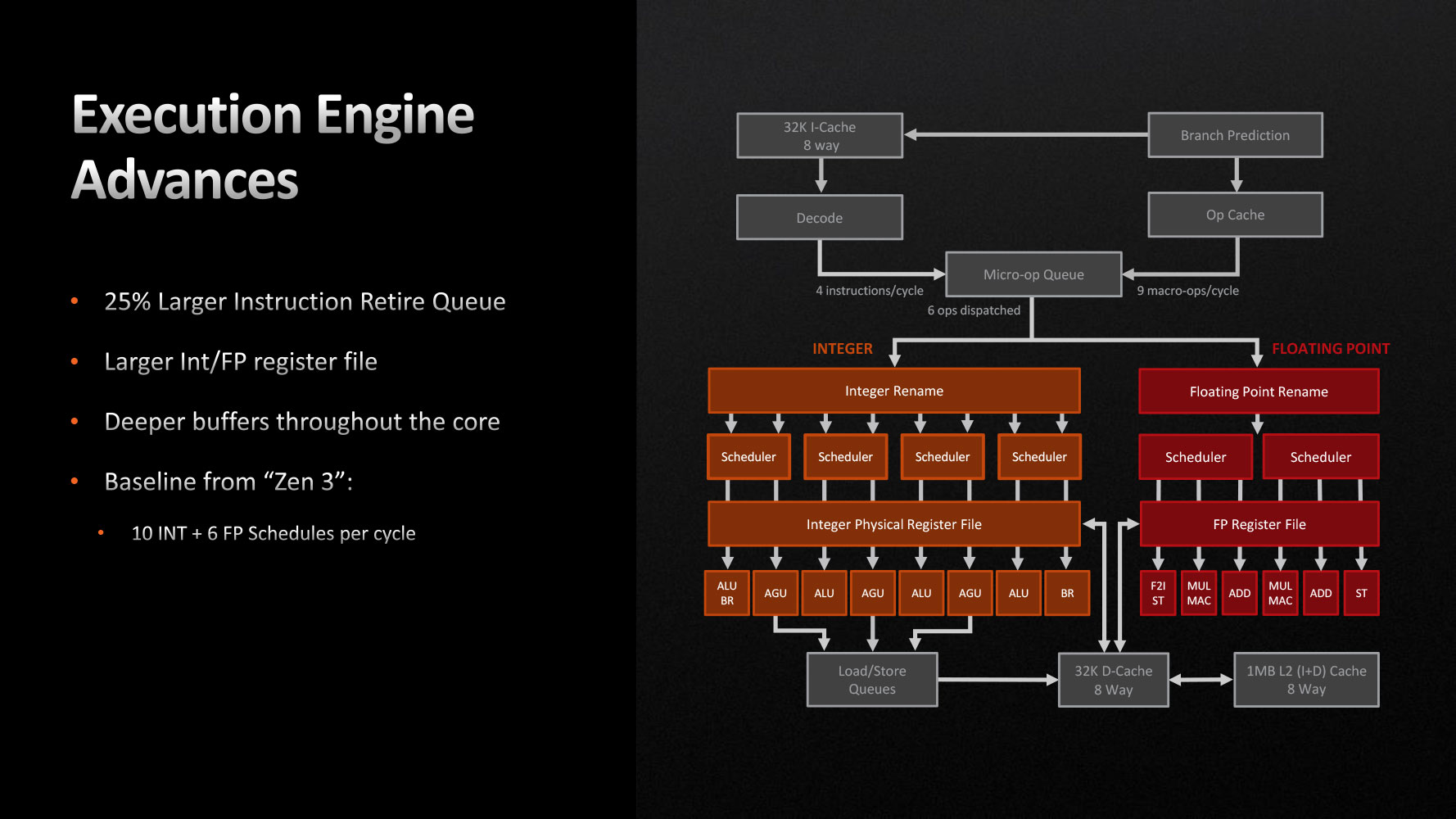
The Execution Stage is the main number-crunching machinery, and broadly features two components for the kind of math workload being executed—Integer and Floating Point. The "Zen 4" execution stage features a 25% larger instruction retire queue, larger register files, and higher buffer queue-depths throughout the core.

With "Zen 4," AMD is introducing support for AVX-512, in a bid to increase the processor's AI inferencing performance. The company did this in a die-area efficient, and energy-efficient manner, with no impact on CPU core frequency. AVX-512 operations are executed on a dual-pumped 256-bit FPU, rather than building ground-up 512-bit FP machinery. VNNI and Bfloat16 instruction-sets are also added, which mean that "Zen 4" can handle pretty much all of the AVX-512 client-relevant workloads that competing Intel processors can.


The Load/Store unit is the part of the core that interfaces with the memory sub-system. The "Zen 4" core gets a 22 percent larger Load Queue, with improved data-port conflict-resolution. There's a 50% larger L2 data transition lookaside buffer. The cache-hierarchy of the Ryzen 7000 desktop processor is similar to that of Ryzen 5000, with a few key differences, besides bandwidth/latency improvements—the dedicated L2 cache has been doubled in size to 1 MB per core. The eight CPU cores on a CCD share a monolithic 32 MB L3 cache, with uniform access to each core.
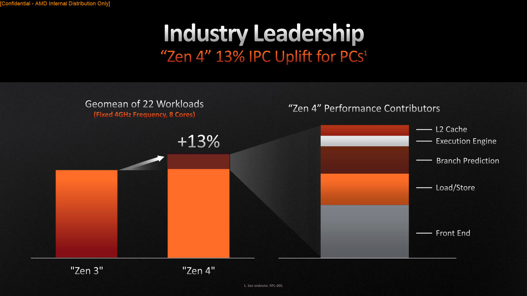
These improvements contribute to a 13 percent IPC improvement over "Zen 3," AMD claims. The company provided a break-up of which components are contributing to the IPC uplift, and we see that close to two-thirds of it are coming from improvements to the front-end and load/store stages. Branch prediction improvements contribute a fifth of this uplift. Interestingly, the L2 cache contributes barely 1/10th of the IPC uplift, in the tested applications—we believe this increase is mostly relevant for server applications where it should be able to make a difference. Intel's "Golden Cove" P-core comes with 1.25 MB L2 cache, and "Raptor Cove" features 2 MB. Despite the doubling in L2 cache sizes, the resulting increase in cache latency is very well contained (from 12 cycles on the 512 KB L2 of "Zen 3," to just 14 cycles on "Zen 4").
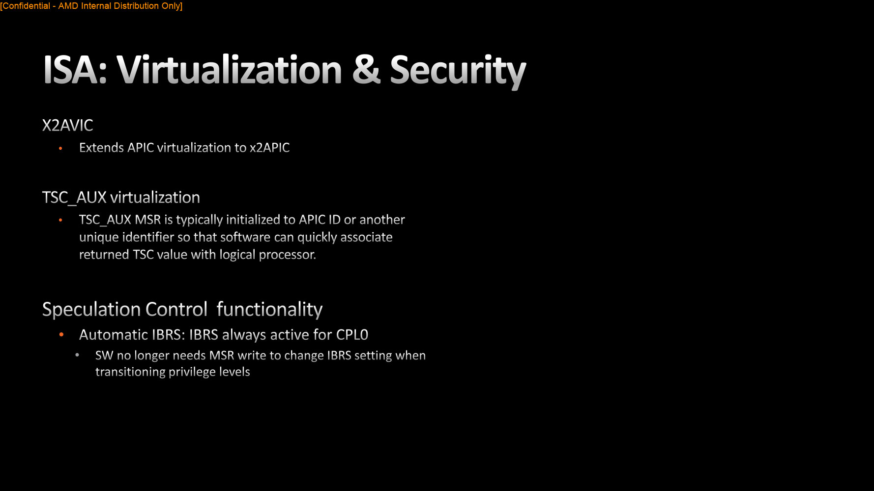
VBS (virtualization-based security) is the standard on new Windows 11 installs and gets activated automatically, unless you specifically disable it. Windows 11 Security Center already flags VBS not being enabled as a warning, similar to Antivirus being disabled or outdated. AMD made several improvements to the Virtualization feature-set, to reduce its performance impact in a VBS-enabled client environment. This includes speculation control, dual AVIC to go with the physical dual-APIC, and TSC_AUX virtualization.
New 6 nm IO Die

Ryzen 3000 "Matisse" and Ryzen 5000 "Vermeer" processors featured a cIOD built on the 12 nm FinFET Global Foundries node, but with Ryzen 7000 "Raphael," AMD is taking a giant leap toward improving the power characteristics of the cIOD, by building it on the new 6 nm TSMC node. This was needed mainly because the cIOD now packs an RDNA 2 iGPU, besides the higher bandwidth switching fabric of the DDR5 and PCIe Gen 5 interfaces also warranting the change. The 12 nm previous-gen cIOD TDP was already estimated to be up to 15 W, and the addition of an iGPU would've thrown things off gear. In addition to 6 nm, AMD is deploying several of the power-management features of the Ryzen 6000-series "Rembrandt" mobile processor on this cIOD, which mainly have to do with aggressive power management and rapid sleep/wake for the various components on the die.
The new 6 nm cIOD packs a dual-channel DDR5 memory controller (4x 40-bit channels, including ECC and hardware-accelerated encryption support), with native support for DDR5-5200; a PCI-Express 5.0 x28 root-complex; a USB 3.2 controller with support for 20 Gbps 2x2 ports, USB-C, and DisplayPort passthrough from the iGPU. AMD was very clear that the inclusion of an iGPU doesn't make "Raphael" an APU, because the iGPU is rather basic, just about enough for non-gaming workloads. The company intends to continue making APUs—processors with beefy iGPUs for mainstream gaming performance—including for the desktop platform. Full ECC support on desktop is technically possible, but it will depend on the motherboard manufacturers—AMD isn't doing anything to prevent them from making their boards ECC compatible.

The Radeon 610 iGPU is based on the RDNA 2 graphics architecture, and packs just two Compute Units, which work out to 128 stream processors. The Display CoreNext (DCN) and Video CoreNext (VCN) components are of modern design. The VCN offers hardware-accelerated AV1 and H.265 decode, as well as hardware-accelerated H.265 encode. Just to clarify, there is hardware AV1 decode support, but no encode, which isn't a big deal at all. In terms of monitors, the DCN supports DisplayPort 2.0 UHBR10, HDMI 2.1 with FRL, and DisplayPort passthrough for the USB type-C ports connected to the on-die USB 3.2 controller. When paired with a discrete graphics card on Windows 10 or Windows 11, the iGPU supports Hybrid graphics, much in the same way as it's implemented on notebooks. You plug in your monitor to the iGPU, and it wakes up your discrete GPU (graphics card) when needed. The RDNA 2 compute units are of the same kind you'd find in Radeon RX 6000 series GPUs, including ray tracing support, but this is of no use on the Radeon 610. The only reason AMD went with RDNA 2 is because it can offer comparable levels of performance with just two CUs, to a "Vega" based iGPU that would need more CUs (thereby increasing die-size).

As we mentioned earlier, AMD needed a new socket as it was transitioning to DDR5 and PCIe Gen 5, which come with stiff physical-layer signaling requirements that AM4 couldn't provide. AM5 also makes processors "future-ready" as it enables two-way communication with the voltage regulators. The added pin-count was needed not just for DDR5 and its 40-bit sub-channels, but also for four additional PCIe lanes. The processor puts out a total of 28 PCIe Gen 5 lanes. 16 of these are meant for PEG (graphics card slots); 4 serve as chipset bus, and 8 lanes are available for the motherboard vendors to play around with: either wiring them both out as M.2 Gen 5 x4 slots, or wire one of them as M.2, and use the remaining 4 lanes for high-bandwidth devices, such as discrete USB4 controllers, 80 Gbps Thunderbolt 4 controllers, or even CPU-attached low-latency network interfaces. AM5 also significantly increases power-delivery capability over AM4—up to 230 W. The increased power should enable the "Zen 4" cores to run at very high clock-speeds approaching the 6 GHz-mark, or in the future, even enable core-count increases.
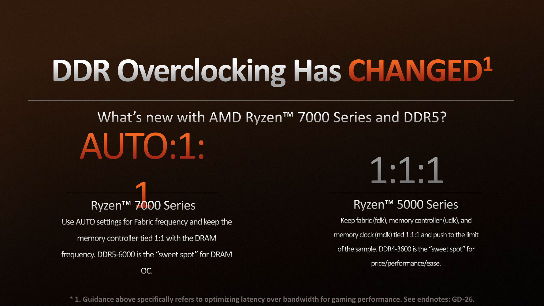
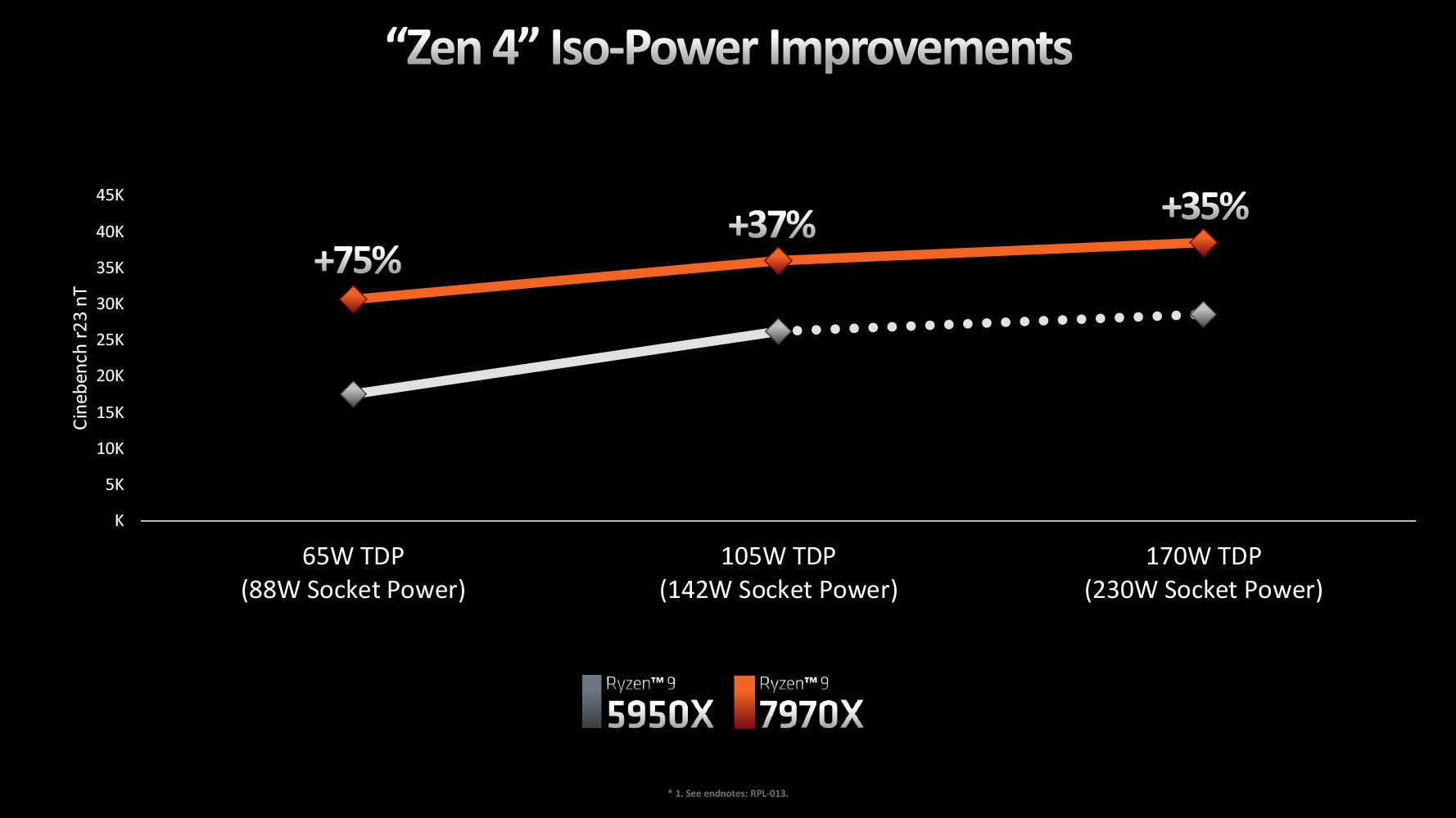
The clock-domains of Ryzen 7000 are similar to those of the Ryzen 5000 series. FCLK defines the Infinity Fabric clock-speed, which is de-linked from UCLK (memory controller clock), and MCLK (DRAM clock). AMD says that DDR5-6000 strikes the "sweetspot" in that this is the highest MCLK you can run while retaining certain memory overclocker optimizations. On Zen 3 you'd want to run Infinity Fabric in sync with memory, but this isn't possible anymore, because FCLK can't reach 3000 MHz (assuming DDR5-6000 memory). Now the optimum config is to run FCLK at 2000, basically a 3:2 divider. Picking "auto" in the BIOS will automatically aim for that setting. Above 6000 MHz, the strategy will be changed to 2:1 ratio.
Apr 25th, 2025 00:01 EDT
change timezone
Latest GPU Drivers
New Forum Posts
- Cracks in my cpu waterblock should I be concerned? (13)
- What's your latest tech purchase? (23595)
- Have you got pie today? (16677)
- Are the 8 GB cards worth it? (177)
- pc randomly blackscreening (0)
- What are you playing? (23462)
- I dont understand the phone OS world..... (49)
- New OLED monitor makes PC unresponsive sometimes (28)
- RTX 5070ti - Which MSRP model has the better/quieter cooler design, ASUS Prime, Gigabyte Windforce or PNY? (7)
- I tried to use AMD Auto Overclock, and now my PC has been freezing up sometimes. Afterwards, the screen goes black or displays artifacts. (29)
Popular Reviews
- NVIDIA GeForce RTX 5060 Ti 8 GB Review - So Many Compromises
- Crucial CUDIMM DDR5-6400 128 GB CL52 Review
- Colorful iGame B860M Ultra V20 Review
- ASUS GeForce RTX 5060 Ti TUF OC 16 GB Review
- Upcoming Hardware Launches 2025 (Updated Apr 2025)
- Sapphire Radeon RX 9070 XT Pulse Review
- Sapphire Radeon RX 9070 XT Nitro+ Review - Beating NVIDIA
- ASRock X870E Taichi Lite Review
- AMD Ryzen 7 9800X3D Review - The Best Gaming Processor
- ASUS GeForce RTX 5080 TUF OC Review
Controversial News Posts
- NVIDIA GeForce RTX 5060 Ti 16 GB SKU Likely Launching at $499, According to Supply Chain Leak (182)
- NVIDIA Sends MSRP Numbers to Partners: GeForce RTX 5060 Ti 8 GB at $379, RTX 5060 Ti 16 GB at $429 (127)
- NVIDIA Launches GeForce RTX 5060 Series, Beginning with RTX 5060 Ti This Week (115)
- Nintendo Confirms That Switch 2 Joy-Cons Will Not Utilize Hall Effect Stick Technology (105)
- Nintendo Switch 2 Launches June 5 at $449.99 with New Hardware and Games (99)
- Sony Increases the PS5 Pricing in EMEA and ANZ by Around 25 Percent (84)
- NVIDIA PhysX and Flow Made Fully Open-Source (77)
- Windows Notepad Gets Microsoft Copilot Integration (75)