 66
66
AMD Ryzen 9 5950X Review
Test Setup »Vermeer Multi-Chip Module
The AMD Ryzen 9 5950X "Zen 3" processor is built on a Socket AM4 multi-chip module package the company refers to as "Vermeer." Since the Ryzen 3000 "Matisse," which was the first desktop processor to implement the 7 nm silicon fabrication process, AMD figured out a way to optimize the utilization of its 7 nm foundry allocation, using two things—building only those components that tangibly benefit from the new node on 7 nm, namely the CPU cores, while moving all other components to a separate die built on older 12 nm process, the cIOD (client IO die). The CPU cores are built on tiny dies with eight cores each, which AMD refers to as the CCD (CPU core die). On the older "Zen 2" microarchitecture, the eight cores were split into two groups of four cores, each, called CPU core complexes (CCX). Each of the two CCX on the "Zen 2" CCD had its own 16-megabyte L3 cache shared between the two cores, and communication between cores of different CCXes required a round-trip to the cIOD.
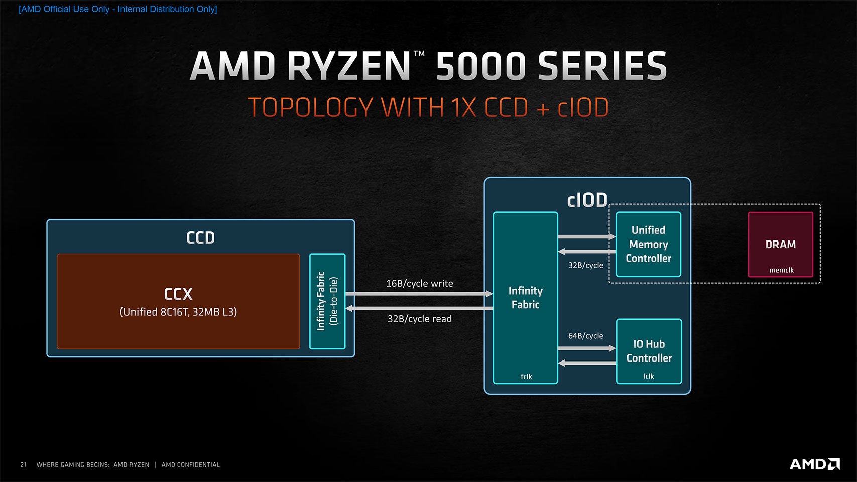
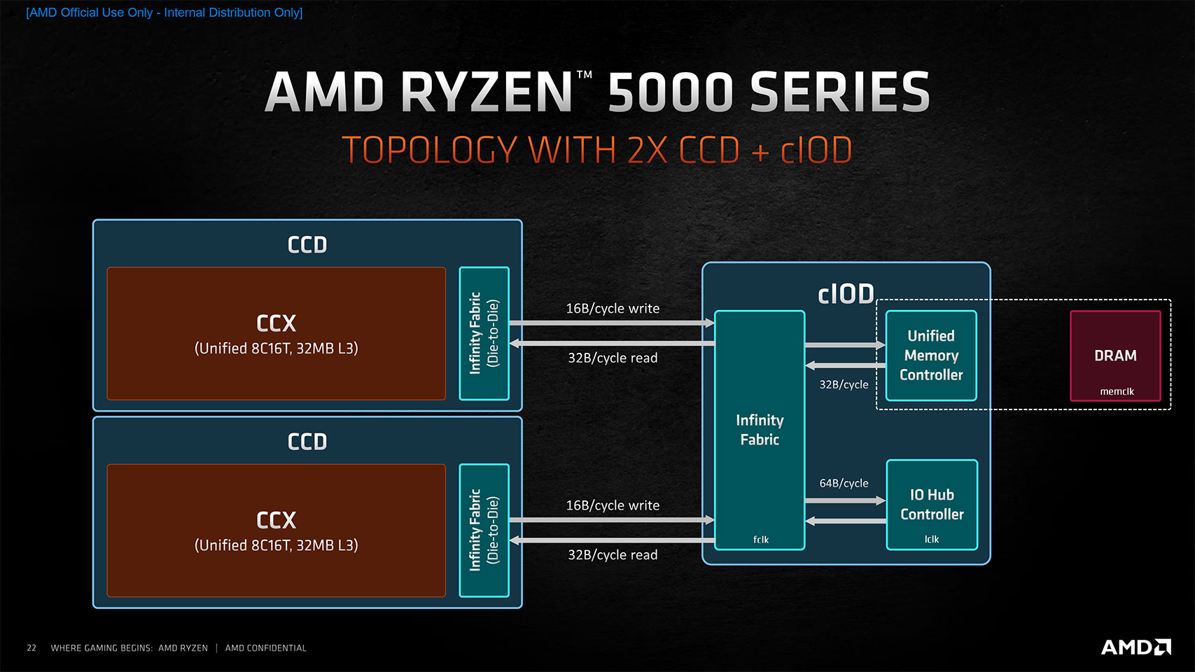
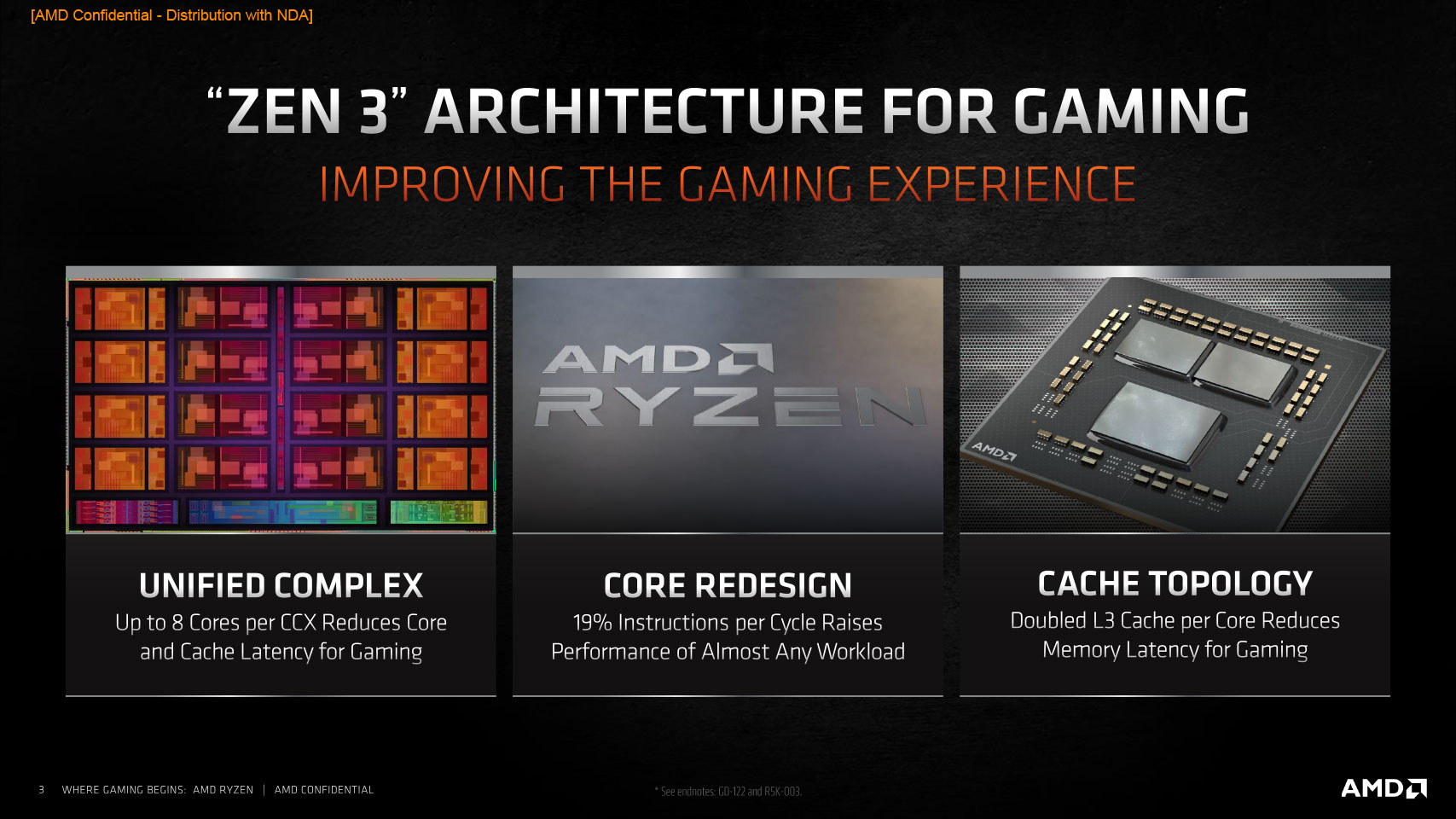
With the new "Zen 3" microarchitecture, the biggest high-level change with the CCD is AMD's enlargement of the CCX to now include up to eight cores (essentially taking up the whole CCD). There's now one 8-core CCX per CCD. The biggest dividend of this change has to be improved inter-core latency as the eight cores now share the same L3 cache; the other big dividend has to be cache size. Each core on the CCD now has access to the full 32 MB L3 as a victim cache, so lightly threaded workloads should see a performance uplift. 8-core Ryzen 7 5000-series models, such as the 5800X, feature a single CCD with all its cores enabled. 6-core parts, such as the Ryzen 5 5600X, feature one CCD with any two of its cores disabled (shouldn't matter which ones). The 12-core Ryzen 9 5900X and 16-core Ryzen 9 5950X are parts that have two 8-core CCDs besides the cIOD. The 5900X is carved out by disabling any two cores per CCD, while the 5950X has all cores enabled on both CCDs. We confirmed with AMD that Ryzen 5000 "Vermeer" uses the same exact 12 nm cIOD as the Ryzen 3000 "Matisse," with only a couple of non-physical improvements, such as improved memory clocks and clock domains.
Power Management and Overclocking Enhancements
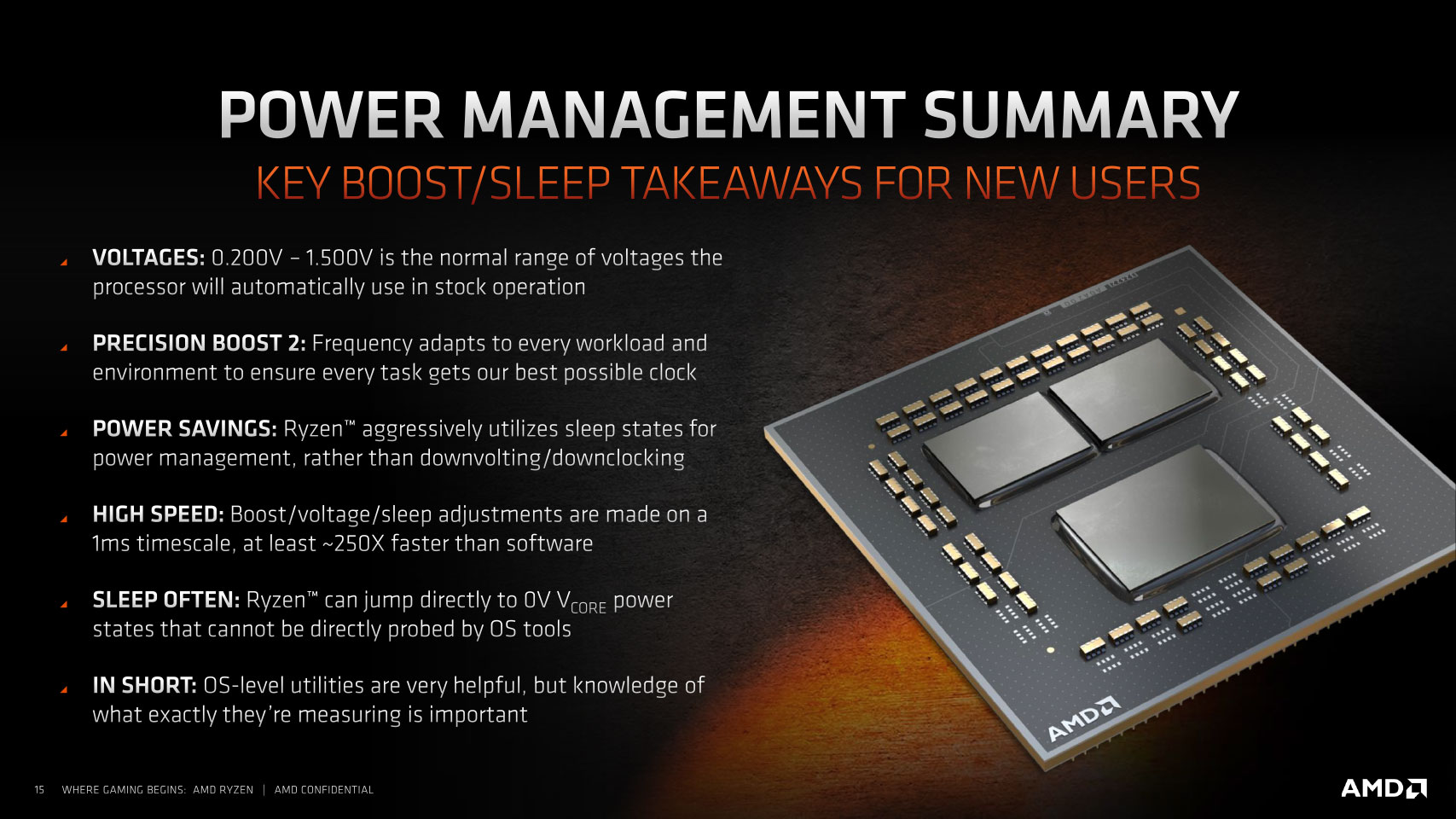
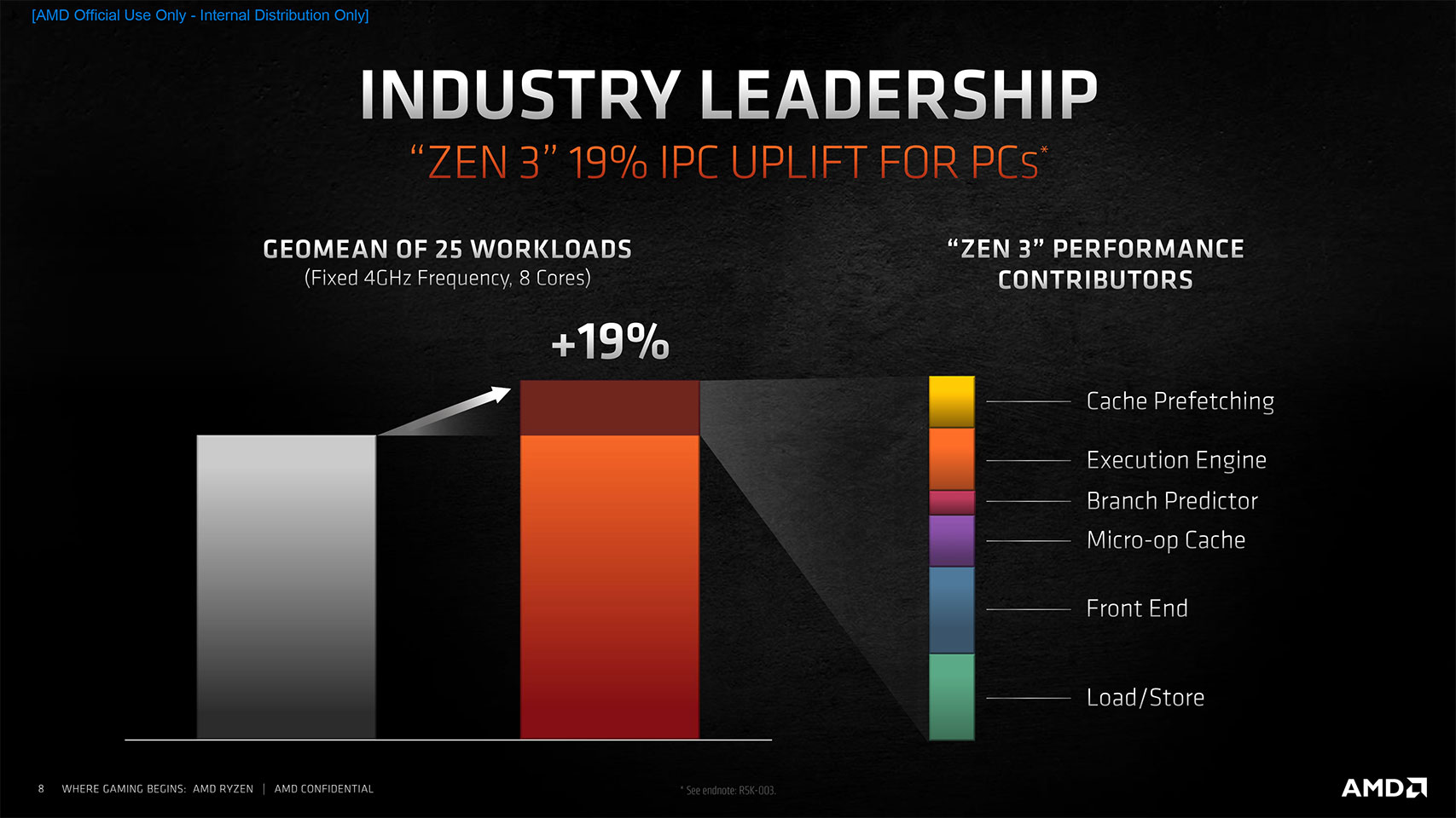
The new Ryzen 5000 "Zen 3" processors are even more independent from the OS than before for power management. The CPUs mostly rely on themselves in gauging processing load and responding with the appropriate performance budget. The "Zen 3" CPU core can operate at voltages ranging all the way from 0.2 V to 1.5 V (normal operation). The same Precision Boost 2 algorithm is used as on "Zen 2" Ryzen 3000 series processors. CPU clock speed boost, voltage adjustments, and clock-gated sleep changes occur at a 1 ms timescale, compared to the 15 ms tick-rate for OS-dictated power management. AMD has also enabled 0 V (power-gated) sleep, with the CPU cores able to jump to power-gated sleep states without being "disturbed" by monitoring tools. Changes have been made to minimize the "observer effect" on CPU cores by monitoring tools.
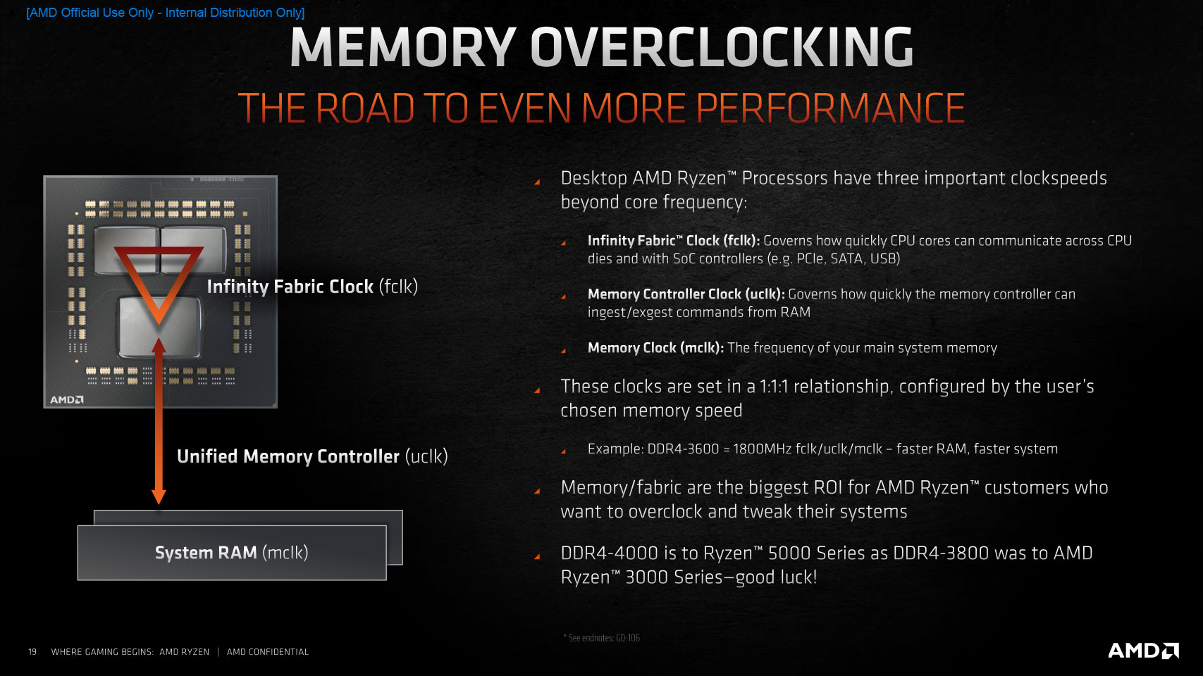
All Ryzen 5000 processors we have thus far reviewed come with unlocked base-clock multipliers, making CPU overclocking a breeze. Memory overclocking is a whole different beast, and efforts have been made to make memory OC easier compared to past generations of "Zen" processors. Unlike on Intel processors, memory overclocking has a greater impact on performance for Ryzen processors, as several other clock domains are tied to the memory clock (mclk), such as the all-important fclk domain, which dictates the frequency at which the Infinity Fabric interconnect operates. We've extensively covered memory overclocking for Ryzen in our definitive memory overclocking guide. Given "Vermeer" uses the same cIOD as "Matisse," the memory controllers are largely unchanged. What's new, however, is that certain Ryzen 5000 series processor models can support DDR4-4000 with a 1:1 fclk:mclk ratio without engaging a 1:2 divider. AMD explained that this is comparable to "some Zen 2 processors can run at 1800 MHz IF, some cannot".
AMD X570 and B550 Chipsets
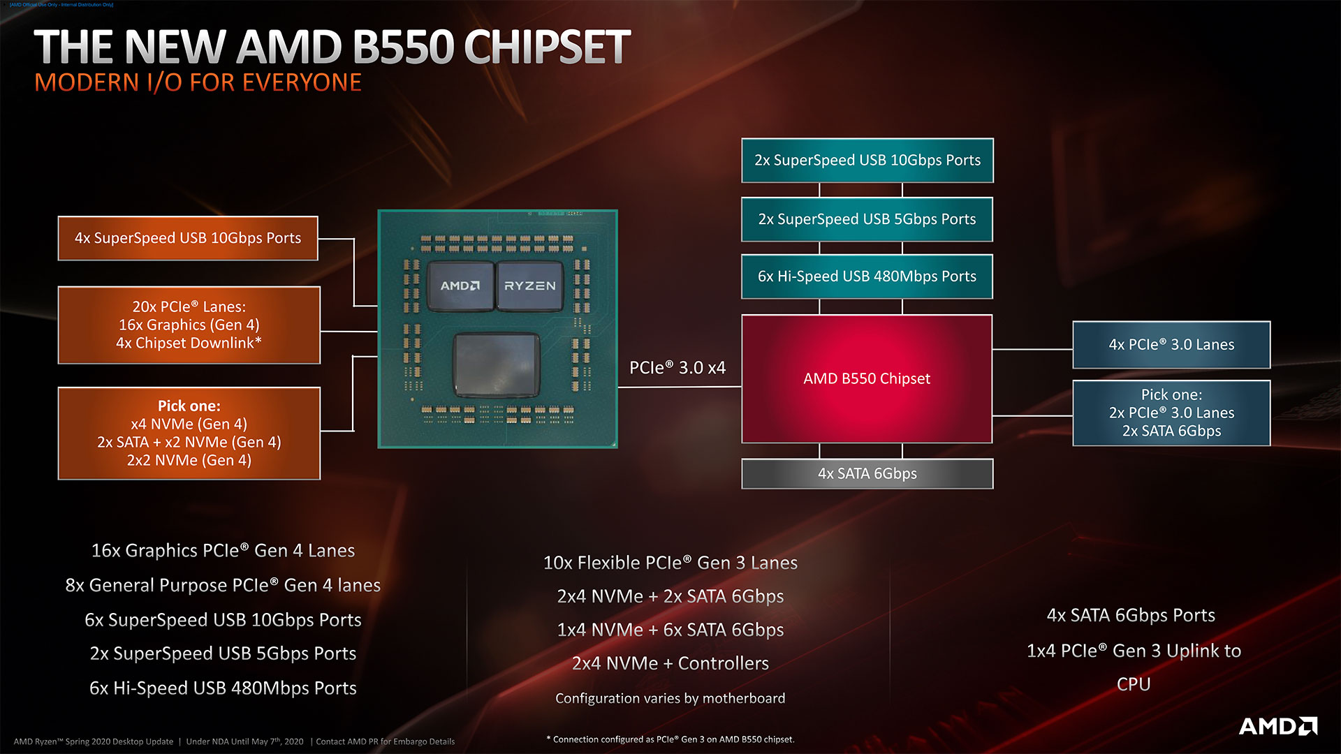
At launch, Ryzen 5000 "Zen 3" processors should be compatible with all Socket AM4 motherboards based on AMD X570 and B550 chipsets, with a BIOS update that has the latest AGESA ComboPI 1.1.0.0 micro-code. The BIOS update must be installed before installing the Zen 3 CPU. Trying to boot the old BIOS with a Zen 3 will not work (we've tried). Luckily, most Socket AM4 motherboards feature some form of USB BIOS flashback feature that lets you update the motherboard BIOS without having installing a processor or memory, which means you won't have to borrow an older processor just to update your motherboard's BIOS. Recent batches of AMD 500-series chipset motherboards should ship with Ryzen 5000 series support out of the box.
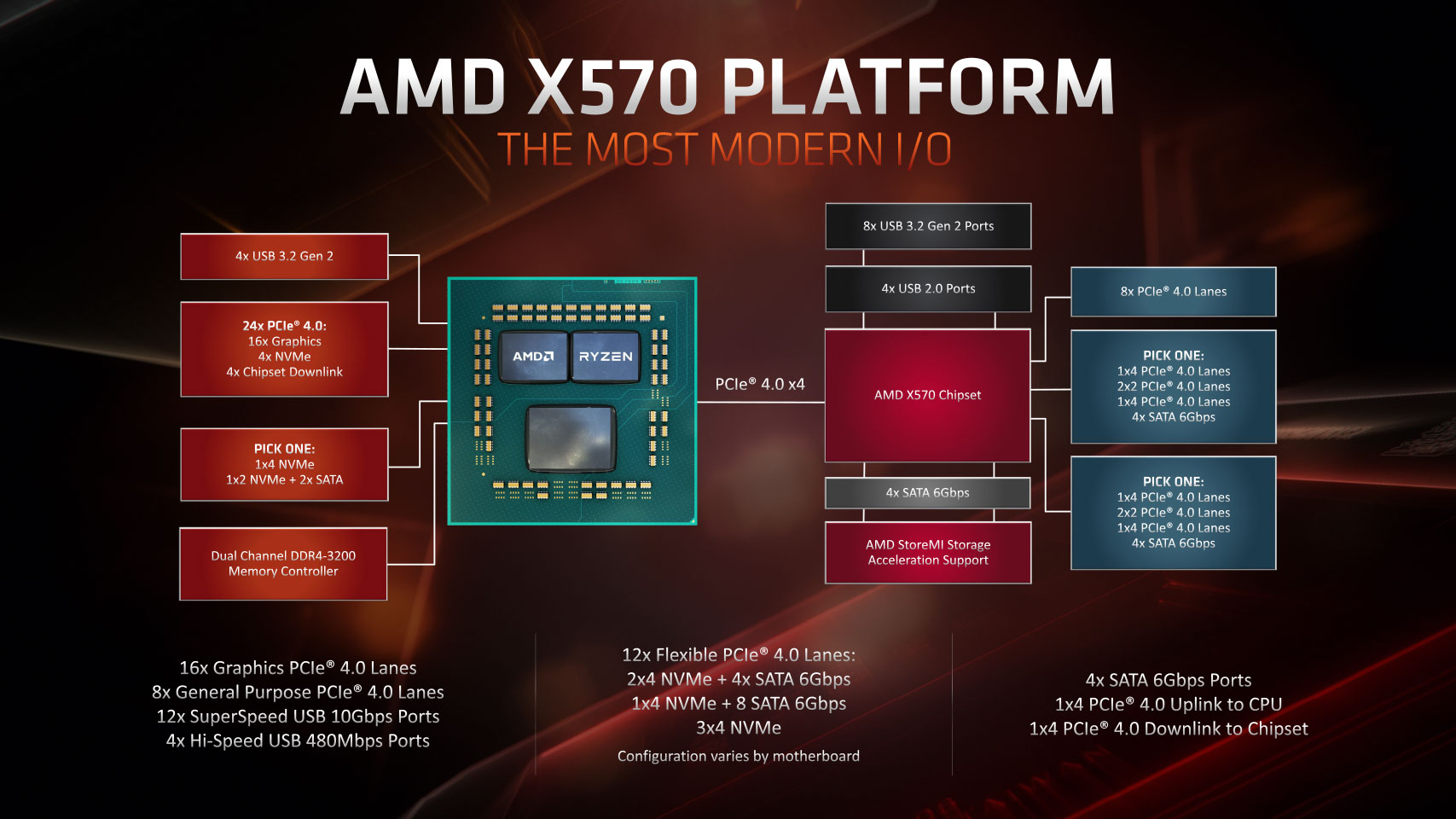
The AMD X570 chipset is a premium offering that enables PCI-Express gen 4.0 not just from the processor (i.e., the main x16 PEG slot and one M.2 NVMe slot), but also downstream PCIe lanes attached to the chipset. You get up to 16 PCIe gen 4 lanes from the chipset, which can be re-configured as SATA or USB3 ports by the motherboard designer. The B550 chipset lets you have one PCIe gen 4 main x16 slot and one M.2 NVMe slot, but all chipset-attached downstream lanes are PCIe gen 3. The B550 puts out eight downstream lanes.
AMD is expected to release a special version of AGESA that enables Ryzen 5000 "Zen 3" support for AMD 400-series chipset motherboards. However, this BIOS update will come with certain riders (e.g., you lose support for older processors). Motherboard vendors are expected to roll out BIOS updates for their 400-series chipset motherboards starting in January 2021.
Apr 25th, 2025 00:08 EDT
change timezone
Latest GPU Drivers
New Forum Posts
- Cracks in my cpu waterblock should I be concerned? (13)
- What's your latest tech purchase? (23595)
- Have you got pie today? (16677)
- Are the 8 GB cards worth it? (177)
- pc randomly blackscreening (0)
- What are you playing? (23462)
- I dont understand the phone OS world..... (49)
- New OLED monitor makes PC unresponsive sometimes (28)
- RTX 5070ti - Which MSRP model has the better/quieter cooler design, ASUS Prime, Gigabyte Windforce or PNY? (7)
- I tried to use AMD Auto Overclock, and now my PC has been freezing up sometimes. Afterwards, the screen goes black or displays artifacts. (29)
Popular Reviews
- NVIDIA GeForce RTX 5060 Ti 8 GB Review - So Many Compromises
- Crucial CUDIMM DDR5-6400 128 GB CL52 Review
- Colorful iGame B860M Ultra V20 Review
- ASUS GeForce RTX 5060 Ti TUF OC 16 GB Review
- Upcoming Hardware Launches 2025 (Updated Apr 2025)
- Sapphire Radeon RX 9070 XT Pulse Review
- Sapphire Radeon RX 9070 XT Nitro+ Review - Beating NVIDIA
- ASRock X870E Taichi Lite Review
- AMD Ryzen 7 9800X3D Review - The Best Gaming Processor
- ASUS GeForce RTX 5080 TUF OC Review
Controversial News Posts
- NVIDIA GeForce RTX 5060 Ti 16 GB SKU Likely Launching at $499, According to Supply Chain Leak (182)
- NVIDIA Sends MSRP Numbers to Partners: GeForce RTX 5060 Ti 8 GB at $379, RTX 5060 Ti 16 GB at $429 (127)
- NVIDIA Launches GeForce RTX 5060 Series, Beginning with RTX 5060 Ti This Week (115)
- Nintendo Confirms That Switch 2 Joy-Cons Will Not Utilize Hall Effect Stick Technology (105)
- Nintendo Switch 2 Launches June 5 at $449.99 with New Hardware and Games (99)
- Sony Increases the PS5 Pricing in EMEA and ANZ by Around 25 Percent (84)
- NVIDIA PhysX and Flow Made Fully Open-Source (77)
- Windows Notepad Gets Microsoft Copilot Integration (75)