 99
99
Intel Core i3-12300 Review - World's Fastest Quad-Core
Unboxing & Photos »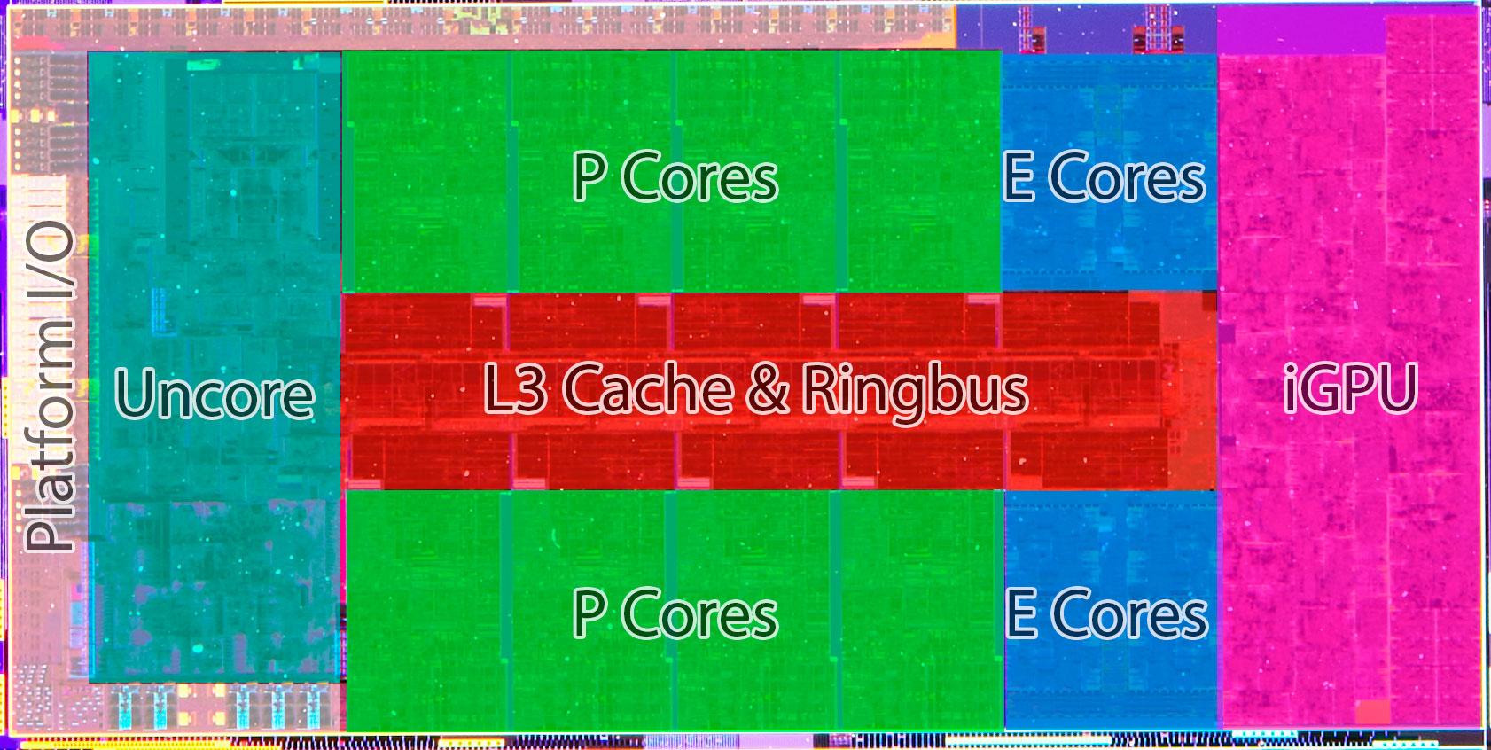
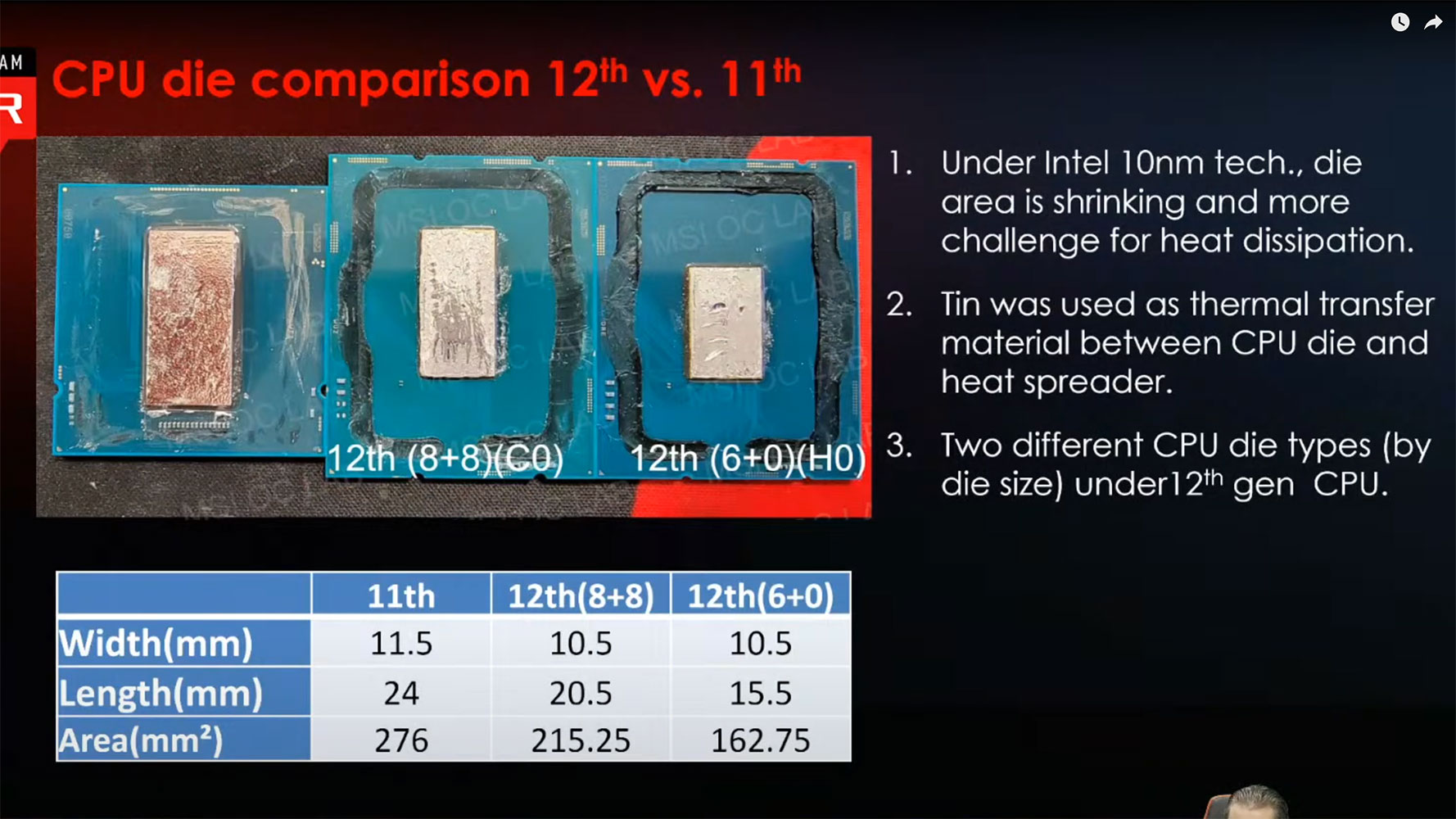
Intel paper-launched the 12th Gen Core processor family on October 27, allowing us to post everything about the processor except performance testing, so we did a more comprehensive Preview Article on the "Alder Lake" microarchitecture. The Core i3-12300 is based on a physically smaller die than the C0 die of the the i9-12900K, codenamed "H0." There are no die-shots from Intel of this die, but MSI OC Lab de-lidded a Core i5 "H0" processor and compared its die-size with that of the larger die. Built on the same Intel 7 node as the C0 die, formerly known as 10 nm Enhanced SuperFin, the new H0 die is about 24% smaller in area. Considering these are high-volume SKUs, that's a massive savings in wafer consumption at scale.
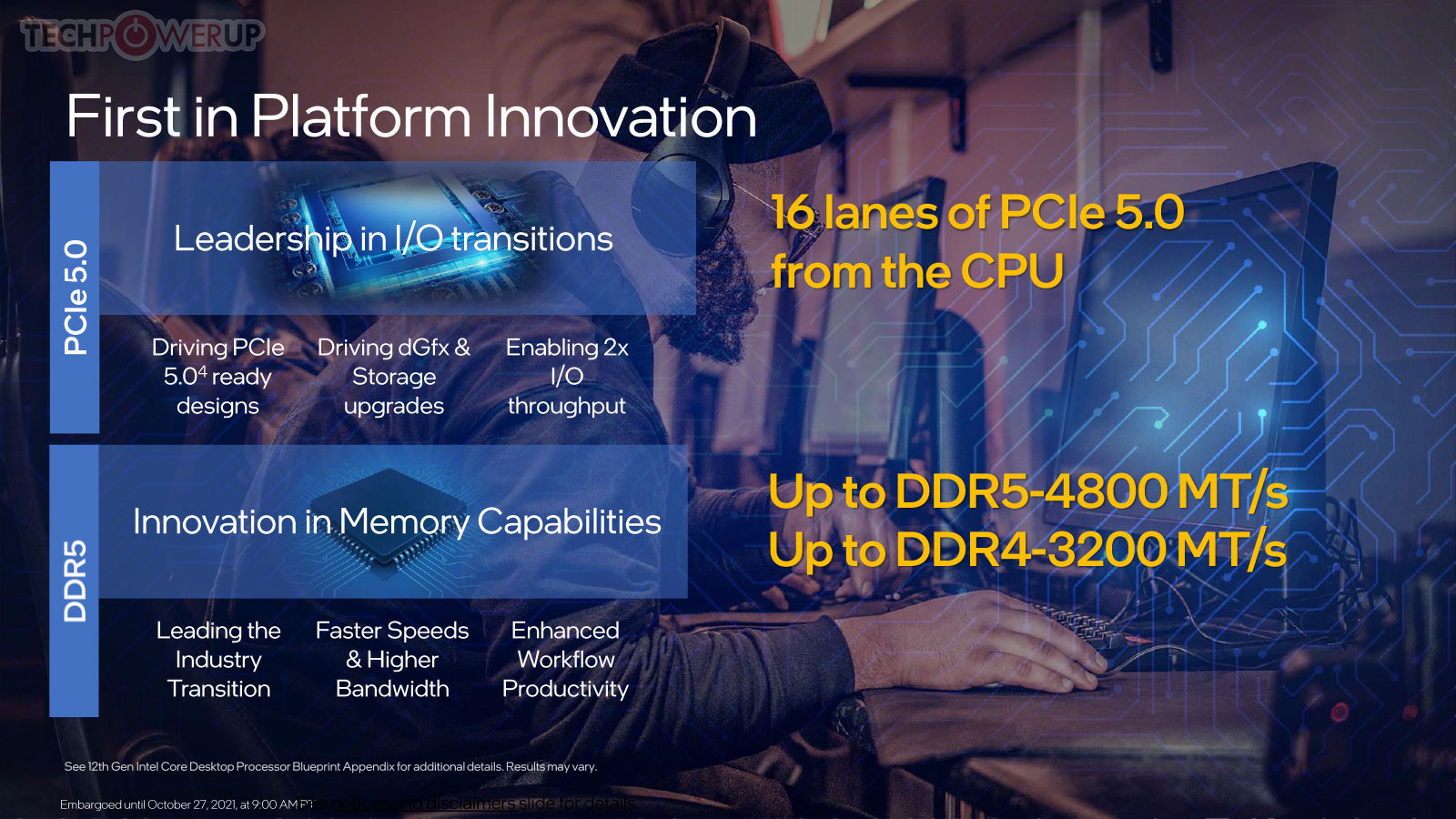
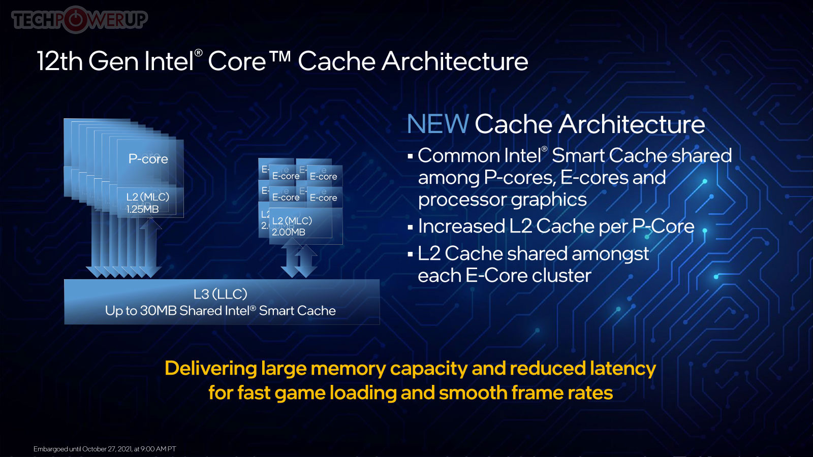
Unlike the C0 die, which physically features 8 "Golden Cove" P-cores and 8 "Gracemont" E-cores, the H0 silicon lacks E-cores and physically only has 6 "Golden Cove" P-cores. With the E-core clusters and a couple of P-cores out of the way, the shared L3 cache size is proportionately reduced to 18 MB. The uncore (integrated northbridge), Xe-LP graphics core, and I/O interfaces are the same as the C0 die. You get 16 lanes of PCI-Express Gen 5 which go toward the PEG slot, 4 lanes of PCI-Express Gen 4 toward a CPU-attached M.2 NVMe slot, and 8 DMI Gen4 lanes toward the chipset bus. The Core i3-12300 only features four active P-cores out of the six on the die, and the shared L3 cache size is cut down to 12 MB.
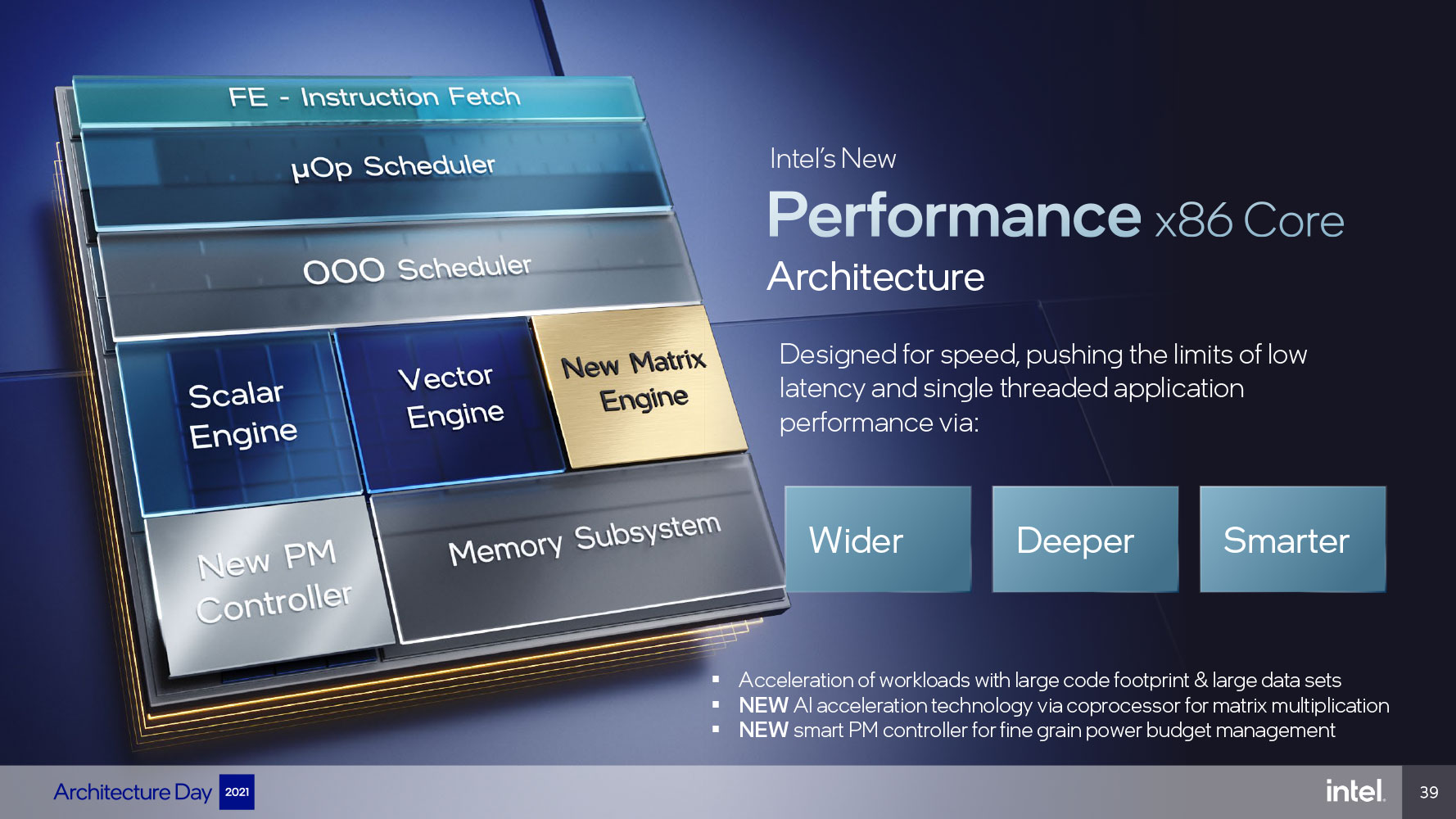
The "Golden Cove" performance core (P-core) features numerical increments to the decode unit, micro-op queue, and micro-op cache. The out-of-order (OoO) engine sees similar increments with 6-wide allocation and 12-wide execution ports, compared to 5-wide allocation and 10-wide execution ports for Cypress Cove. The execution stage sees the addition of a fifth execution port and ALU, FMA with FP16 support, and an updated fast adder (FADD). Similar improvements are made to the cache and memory sub-system. These add toward the 28% IPC uplift for this core.
There are no E-cores physically present on the H0 silicon. With no Hybrid CPU Core architecture present, the Core i3 H0 processor is a traditional multi-core processor that doesn't quite need the Intel Thread Director middleware, although we don't know if Thread Director is absent on these chips or a vestige of it is present.
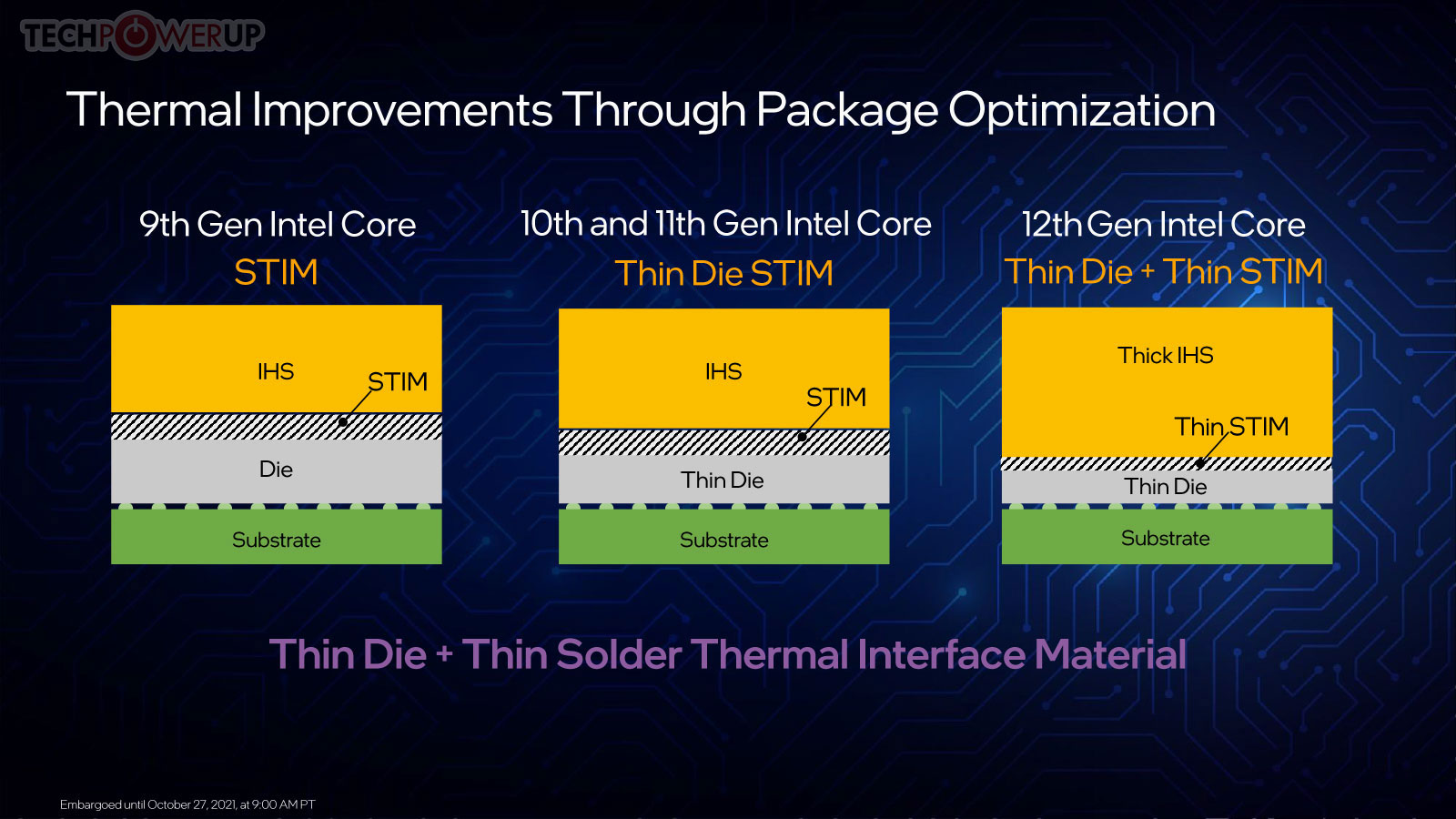
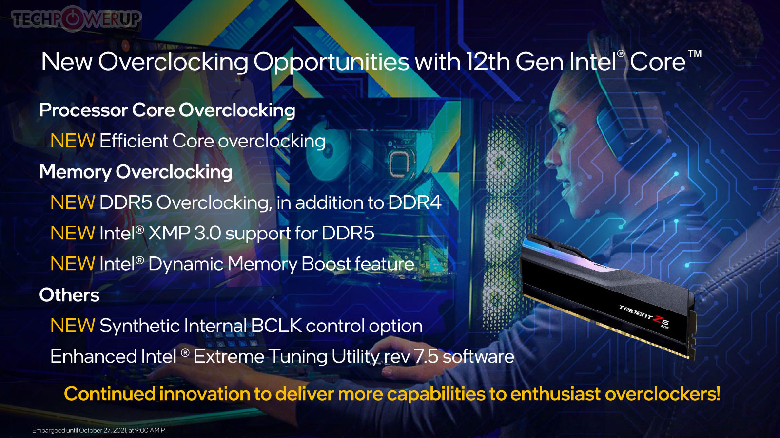
To eke out the best-possible thermals from the 14 nm node it was stuck with, Intel pulled off some innovative ways to transfer heat between the silicon and cooling solution over the past couple of solutions. These innovations continue with "Alder Lake." The die and STIM are now thinner, and the copper IHS thicker. Among the new overclocking capabilities are the ability to tweak even the E-cores, DDR5 memory, new XMP 3.0 profiles for DDR5 memory, synthetic BCLK that ensures a base-clock overclock doesn't break sensitive clock domains relying on it, and external clock generation, in addition to the processor's internal clock generator. The Core i3-12300 lacks an unlocked multiplier and hence doesn't offer a multiplier value beyond 44x. You could try playing with the 100 MHz base-clock on a Z690 chipset motherboard, as it is de-coupled with other sensitive clock-domains, such as PCIe.
Intel Z690 Chipset
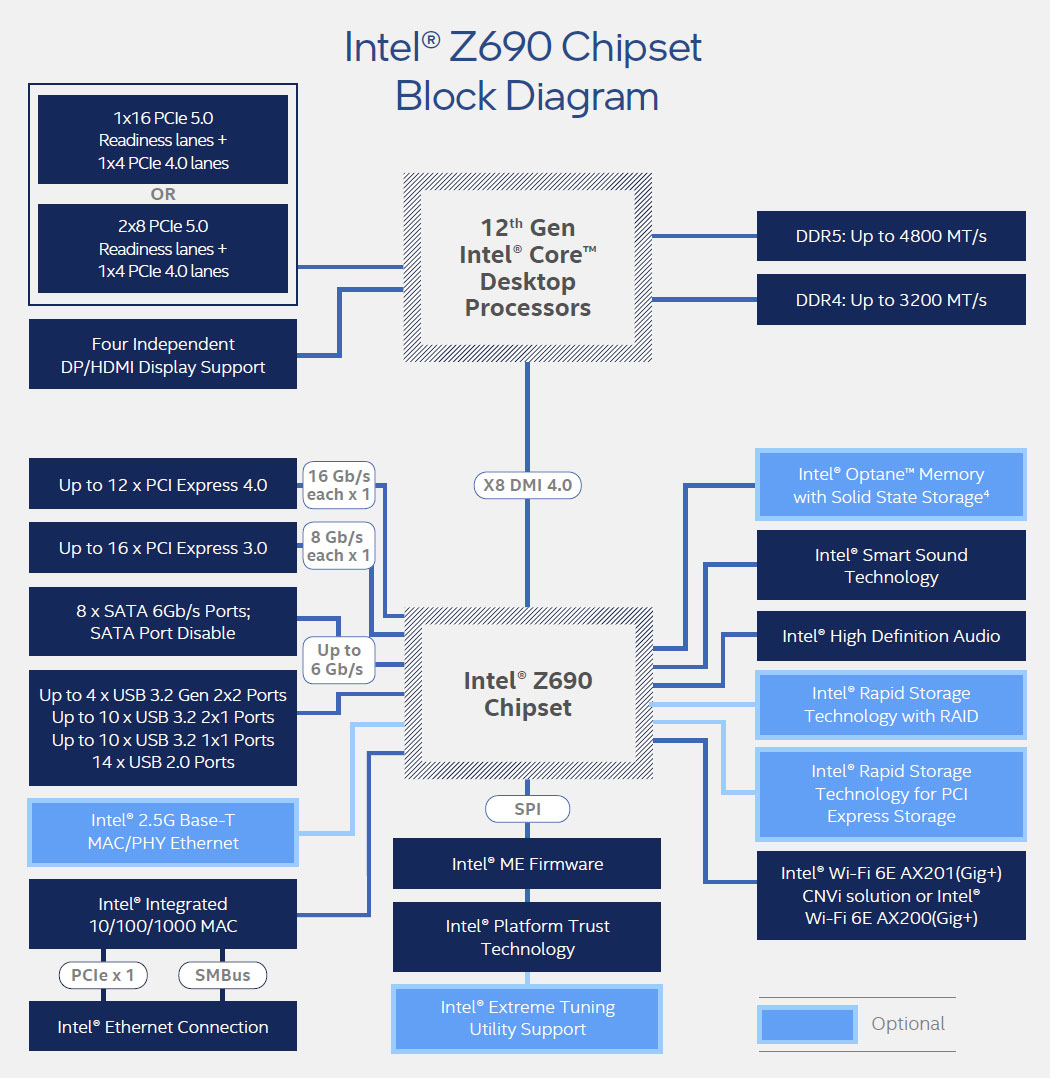
The Z690 chipset is Intel's first client chipset with PCI-Express 4.0 downstream connectivity. It talks to the "Alder Lake-S" processor over the DMI 4.0 x8 chipset bus. Downstream PCIe connectivity includes 12x Gen 4 and 16x Gen 3 PCIe general-purpose lanes. The rest of its chipset-attached connectivity is the same as the Z590, including MIPI SoundWire support, NVMe RAID, 8-port SATA 6 Gbps, and recommended network interfaces that include 2.5 GbE and Wi-Fi 6E.
Intel B660 and H610 Chipsets
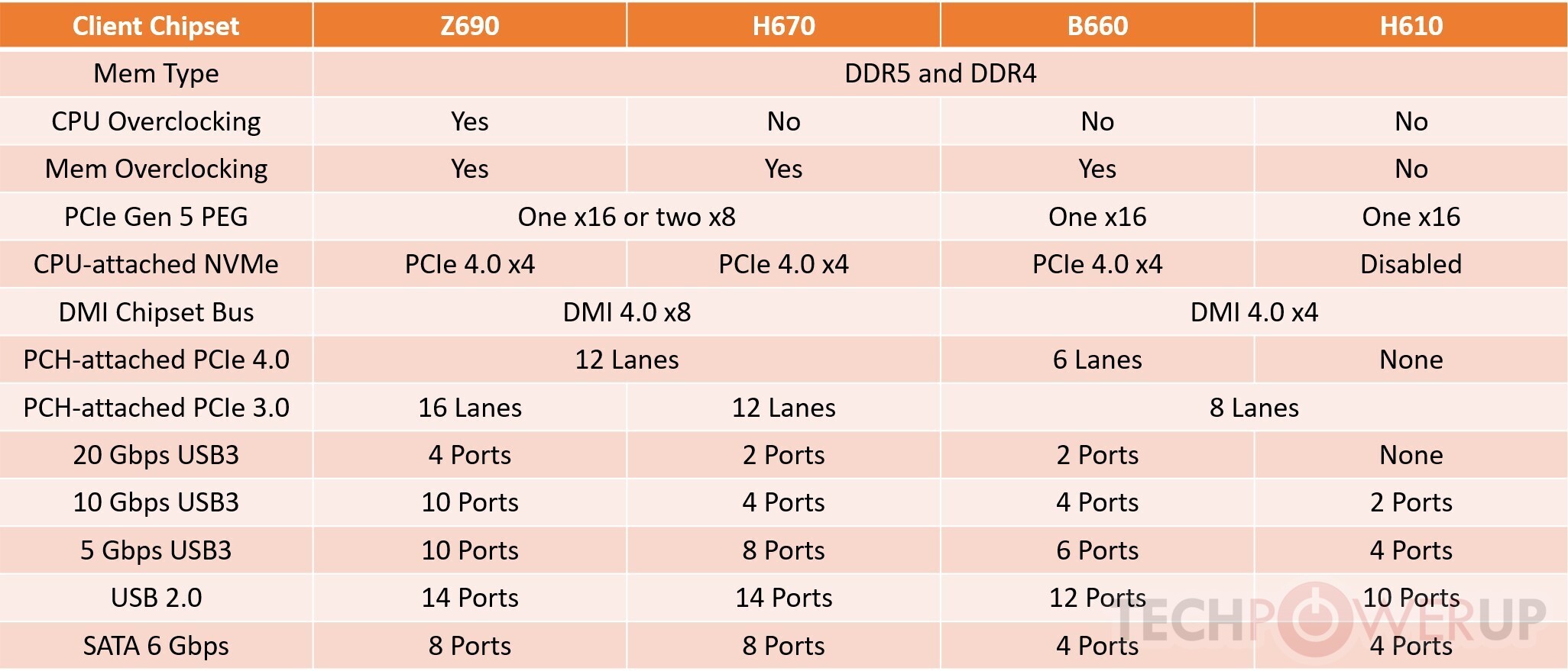
As of this writing, VERY few motherboards use the H670 client chipset, making the B660 Intel's mainstream desktop chipset for those with a "locked" 12th Gen Core processor, those who don't need the I/O options of the Z690 and want to save big on the motherboard. The B660 lacks CPU overclocking support, but permits memory overclocking. Motherboard vendors can choose to give it a PCIe Gen 5 PEG slot, as well as DDR5 memory, although you may come across plenty of motherboards with PCIe Gen4 PEG and DDR4 memory. The B660 chipset uses a narrower 4-lane DMI 4.0 chipset bus than what 12th Gen Core processors are capable of (up to 8 DMI 4.0 lanes). This shouldn't be too much of a problem as the chipset only puts out 6 downstream PCIe Gen4 lanes, besides 8 Gen3 lanes. Motherboard designers should use the downstream Gen4 connectivity to wire out another M.2 Gen4 slot. You also get fewer high-bandwidth USB3 port types. The H610 is the bare entry-level chipset. You lose out on memory overclocking, only get Gen3 PCIe connectivity across the board, and have no CPU-attached NVMe.
Aug 1st, 2025 09:42 CDT
change timezone
Latest GPU Drivers
New Forum Posts
- What CPU should I upgrade to from a 5 3600 to match 7700XT? Upgrade entire platform? (27)
- Are UPS lithium LiFePO4 batteries finally as cheap as lead-acid? (61)
- 3D Printer Club (581)
- 3DMARK "LEGENDARY" (355)
- I just bought an RX570 4Gb (26)
- WB actually did it...They closed Monolith. :( (52)
- PNY 4070 hotspot 107℃ during gaming (18)
- Gigabyte graphic cards - TIM gel SLIPPAGE problem (175)
- Free Games Thread (4825)
- TPU's Nostalgic Hardware Club (20587)
Popular Reviews
- MSI Claw 8 AI+ A2VM Review
- Lenovo Legion 5i (15IRX10) Review - Feature-Rich and Wallet Friendly
- ASUS ROG Crosshair X870E Apex Review
- Herman Miller Logitech G Embody Review - No Pain, No Gain
- Orbital Pathfinder Review
- Montech X5 Review
- Upcoming Hardware Launches 2025 (Updated May 2025)
- Lian Li O11 Dynamic Mini V2 Review
- Noctua NF-A12x25 G2 PWM Fan Review
- AMD Ryzen 7 9800X3D Review - The Best Gaming Processor
TPU on YouTube
Controversial News Posts
- AMD's Upcoming UDNA / RDNA 5 GPU Could Feature 96 CUs and 384-bit Memory Bus (137)
- AMD Radeon RX 9070 XT Gains 9% Performance at 1440p with Latest Driver, Beats RTX 5070 Ti (131)
- Intel "Nova Lake-S" Core Ultra 3, Ultra 5, Ultra 7, and Ultra 9 Core Configurations Surface (110)
- DDR6 Memory Arrives in 2027 with 8,800-17,600 MT/s Speeds (102)
- NVIDIA to Debut GeForce RTX 50-series SUPER GPUs by Christmas (98)
- AMD Sampling Next-Gen Ryzen Desktop "Medusa Ridge," Sees Incremental IPC Upgrade, New cIOD (97)
- Intel CEO Confirms SMT To Return to Future CPUs (95)
- NVIDIA Becomes First Company Ever to Hit $4 Trillion Market-Cap (94)