 59
59
Intel Core i7-12700K Review - Almost as Fast as the i9-12900K
Unboxing & Photos »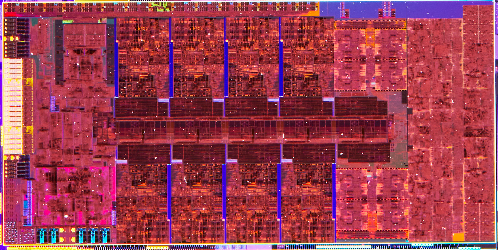
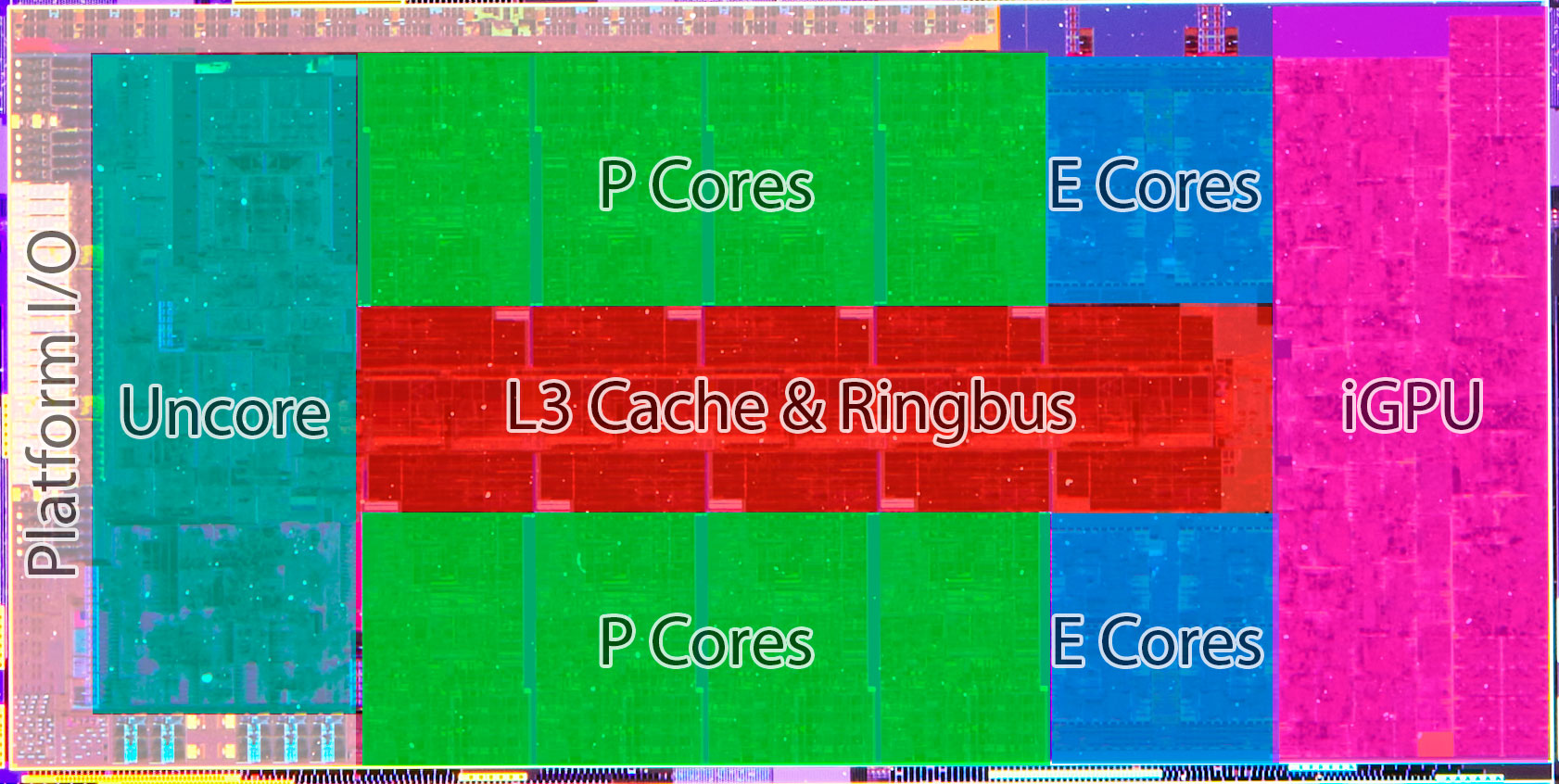
Intel paper-launched the 12th Gen Core processor family on October 27, allowing us to post everything about the processor except performance testing, so we did a more comprehensive Preview Article on the "Alder Lake" microarchitecture. "Alder Lake-S" is the first desktop processor silicon built by Intel on its Intel 7 silicon fabrication node, formerly known as 10 nm Enhanced SuperFin. This node offers transistor-density and power characteristics comparable to 7 nm-class nodes by TSMC. The die measures approximately 200 mm², although it is noticeably smaller than the 14 nm "Rocket Lake-S" die.
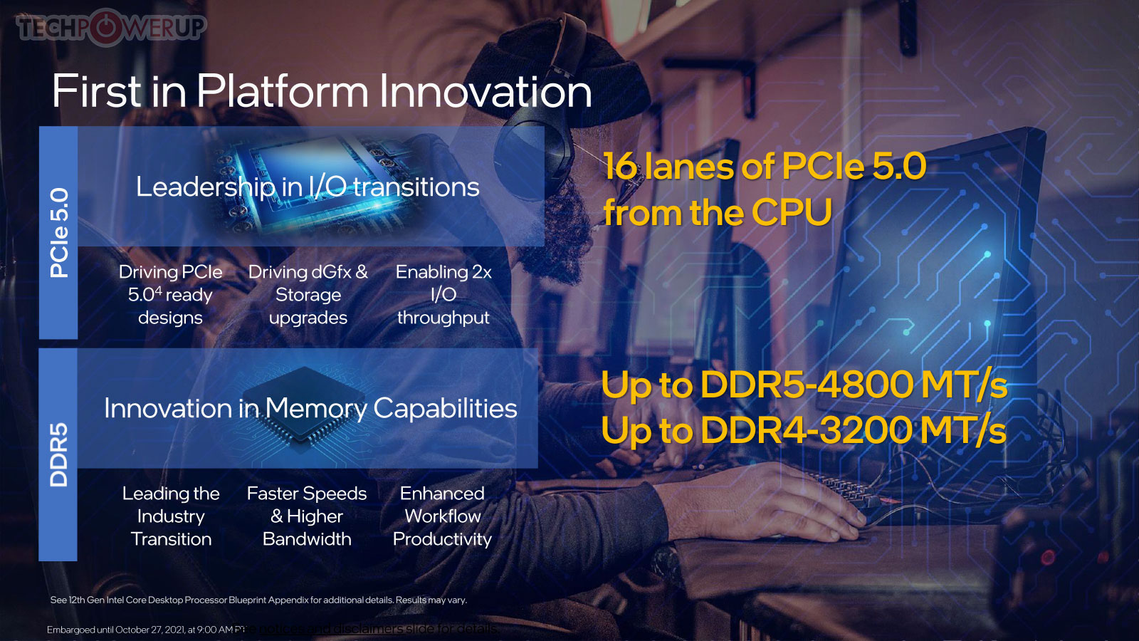
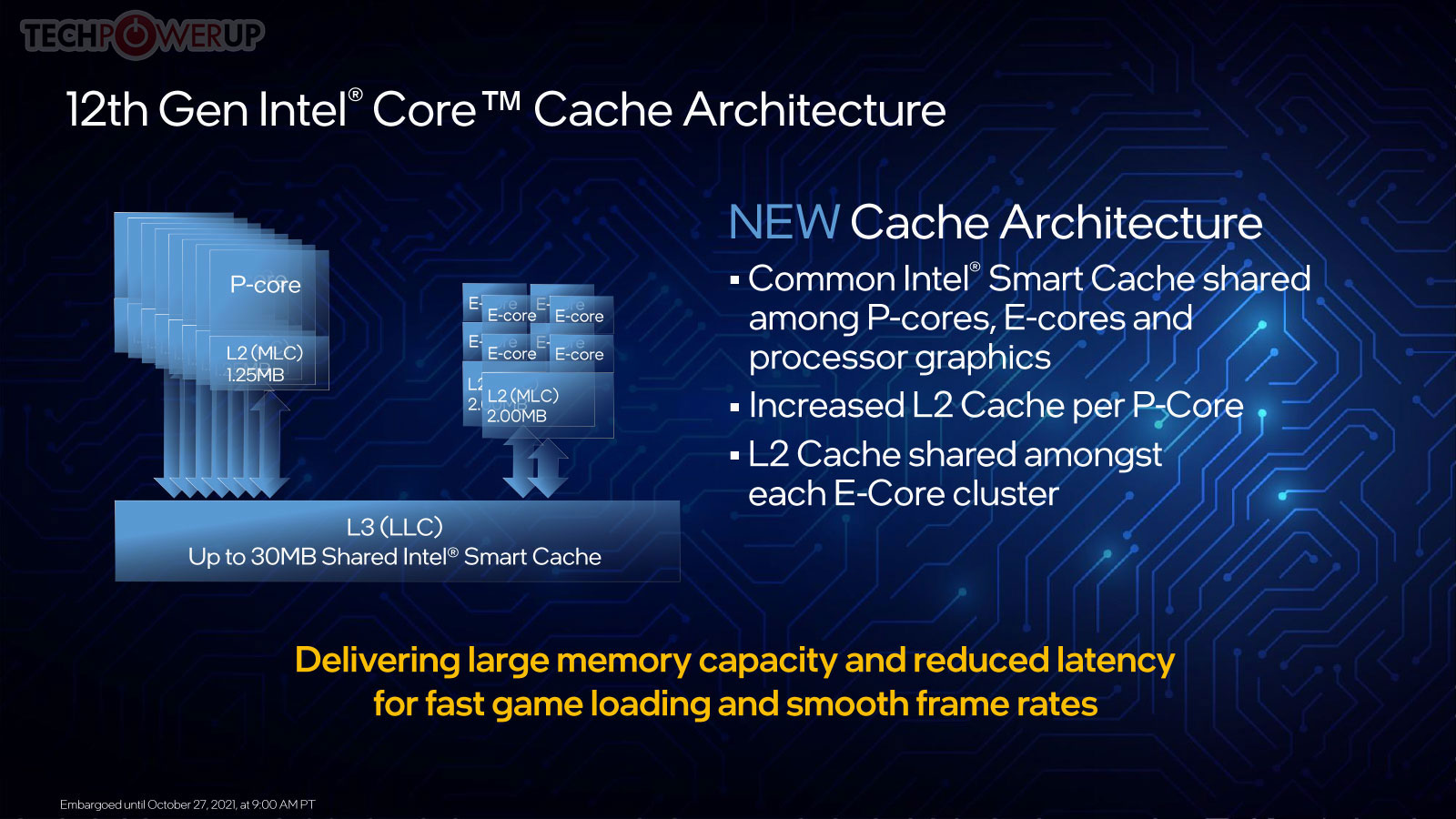
The monolithic silicon features 8 "Golden Cove" P and 8 "Gracemont" E-cores. The E-cores are spread across two 4-core "E-core Clusters." A bi-directional Ringbus and 30 MB of L3 cache connect the P-cores, and E-core clusters, with the Uncore (integrated northbridge) and iGPU. The chip features a dual-mode memory controller that supports 160-bit wide DDR5 (native support for DDR5-4800),or 128-bit wide DDR4 (native support for DDR4-3200). The Gen12 Xe LP iGPU is carried over almost unchanged from the "Rocket Lake-S" silicon, with a minor speed-bump. The PCI-Express root complex is fascinating. The silicon puts out 16 Gen 5 lanes (32 Gbps per lane), which are allocated to the PEG slot on the motherboard; and 12 Gen 4 lanes (16 Gbps per lane) from which four drive a CPU-attached M.2 NVMe slot and eight serve as physical layer of the DMI 4.0 x8 chipset bus (128 Gbps per direction bandwidth).
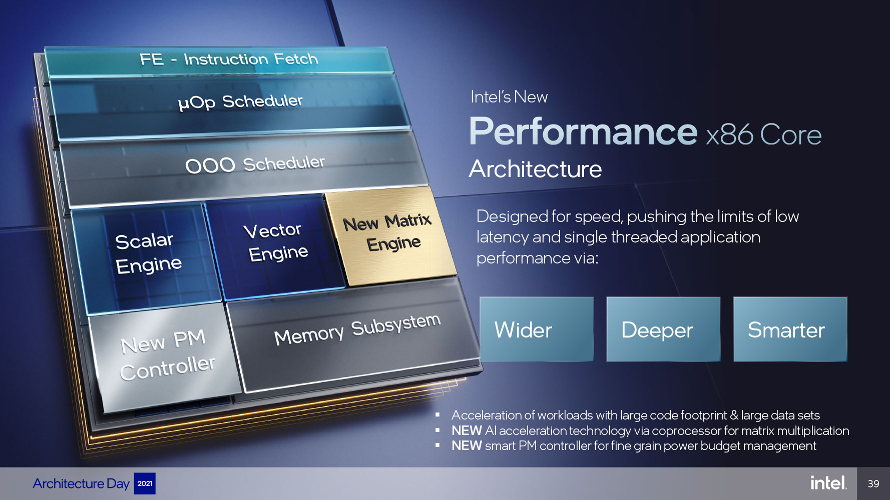

The "Golden Cove" performance core (P-core) features numerical increments to the decode unit, micro-op queue, and micro-op cache. The out-of-order (OoO) engine sees similar increments with 6-wide allocation and 12-wide execution ports, compared to 5-wide allocation and 10-wide execution ports for Cypress Cove. The execution stage sees the addition of a fifth execution port and ALU, FMA with FP16 support, and an updated fast adder (FADD). Similar improvements are made to the cache and memory sub-system. These add toward the 28% IPC uplift for this core. The E-core, on the other hand, is designed to provide a massive performance uplift from the previous-generation "Tremont" low-power microarchitecture, mainly to give it certain ISA capabilities found in larger cores, such as AVX2. The front-end is upgraded by a double-size 64 KB L1 instruction cache, more powerful branch-prediction unit, and two sets of triple out-of-order decoders. The out-of-order engine features a wide 256-entry OoO window and 17 execution ports for more parallelism. The execution stage sees a near 33% increase in both scalar and vector execution stages, as well as double the load store.
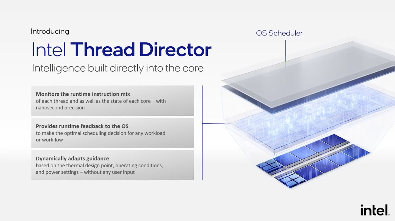
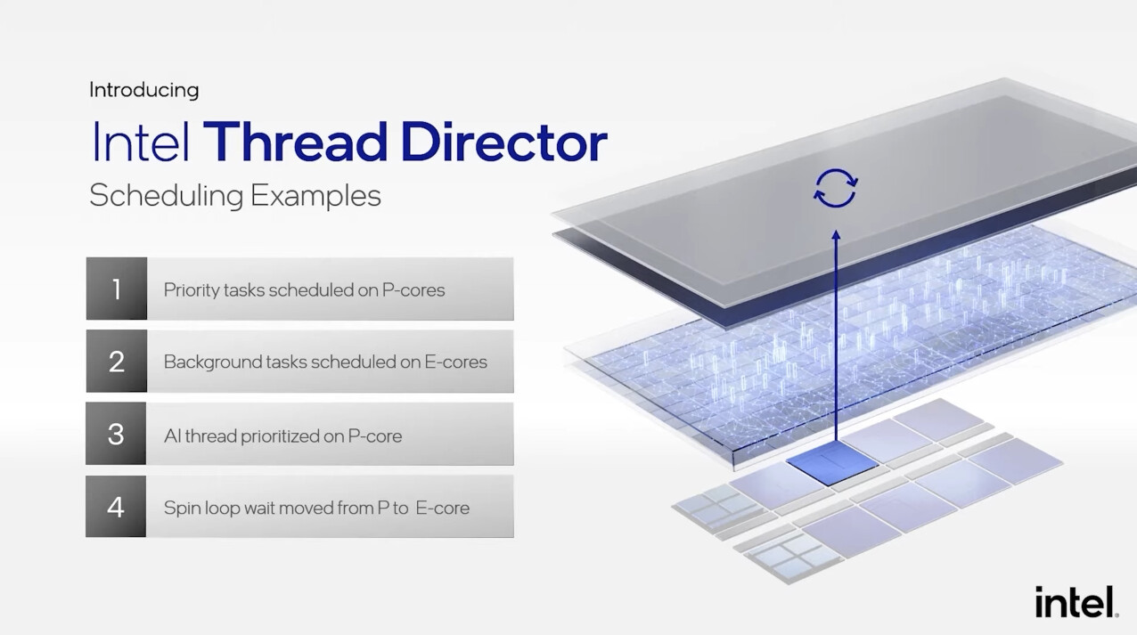
Intel Thread Director is a vital component that ensures the operating system doesn't see Alder Lake as having the same kind of CPU cores, sending processing traffic uniformly to all cores. Instead, it gives the OS a degree of awareness of the Hybrid architecture and ensures certain kinds of tasks are allocated exclusively on P-cores, and others on E-cores. It also senses the nature of the processing workload (whether it's running in the foreground or background), and decides which kind of cores to tie it to. The OS scheduler by itself moves traffic between cores to meet certain power/thermal objectives, but Thread Director ensures this movement doesn't break the core-type hierarchy. Windows 11 is the recommended version of Windows for Alder Lake, as it introduces the ability for software to inform the processor of the nature of its work, and the kind of cores it's comfortable getting processed by.

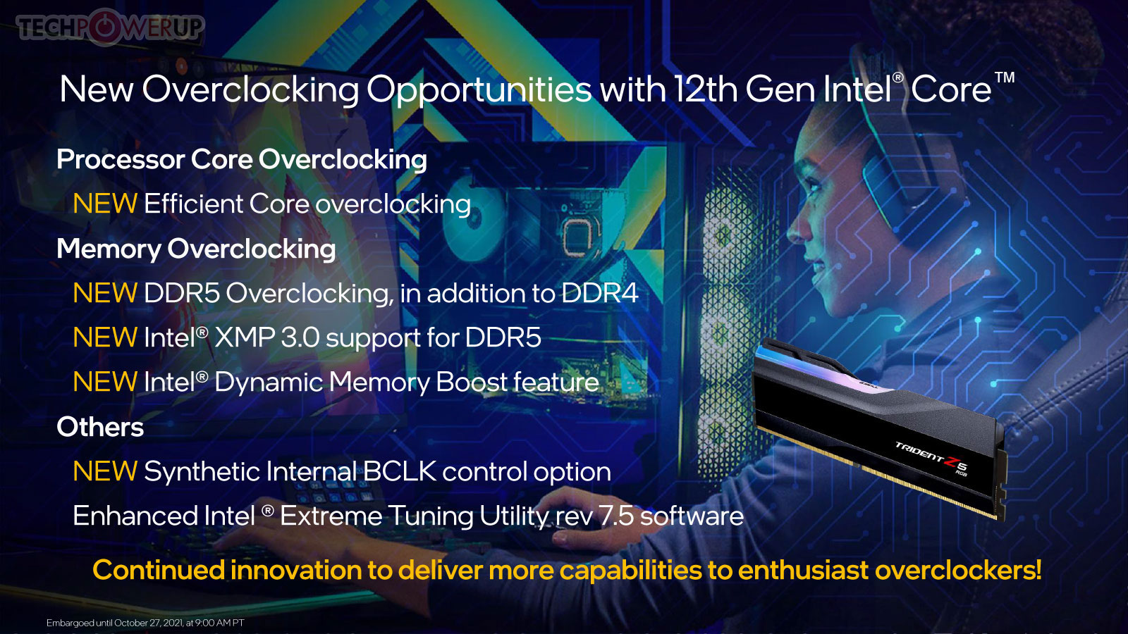
Over the past couple of solutions, Intel pulled off some innovative ways to transfer heat between the silicon and cooling solution to eke out the best possible thermals from the 14 nm node it was stuck with. These innovations continue with Alder Lake. The die and STIM are now thinner, and the copper IHS thicker. Among the new overclocking capabilities are the ability to tweak even the E-cores, DDR5 memory, new XMP 3.0 profiles for DDR5 memory, synthetic BCLK that ensures a base-clock overclock doesn't break sensitive clock domains that rely on it, and external clock generation, in addition to the processor's internal clock generator.


With the monolithic silicon gaining complexity, there are several new overclocking knobs and clock domains to maximize your overclock. The introduction of the E-core adds its own base-clock multiplier, called xE, which works separately from the core ratio of the P-cores, dubbed xP. The xG multiplier dictates iGPU frequency. xR dictates the frequency at which the Ringbus interconnect and L3 cache operate.
Intel Z690 Chipset

Intel is debuting its 12th Gen Core desktop processors in 2021 exclusively with only the unlocked "K" and "KF" variants, so it's only launching the companion Z690 chipset. The "locked" processor SKUs and value-ended chipsets are expected to join the product stack in 2022. The Z690 chipset is Intel's first client chipset with PCI-Express 4.0 downstream connectivity. It talks to the "Alder Lake-S" processor over the DMI 4.0 x8 chipset bus. Downstream PCIe connectivity includes 12x Gen 4 and 16x Gen 3 PCIe general-purpose lanes. The rest of its chipset-attached connectivity is the same as on Z590, including MIPI SoundWire support, NVMe RAID, 8-port SATA 6 Gbps, and the recommended network interfaces that include 2.5 GbE and Wi-Fi 6E.
Jul 30th, 2025 09:36 CDT
change timezone
Latest GPU Drivers
New Forum Posts
- What's your latest tech purchase? (24399)
- RX6800XT Gigabyte Gaming OC not giving image while being on "OC" switch and even sometimes while being on "silent" switch. (21)
- Looking To Make List Of Keyboard Manufacturers (28)
- Spoiler Alert........this car is fast. (255)
- Post your 7-Zip v22.01 scores (438)
- Are UPS lithium LiFePO4 batteries finally as cheap as lead-acid? (53)
- Gigabyte graphic cards - TIM gel SLIPPAGE problem (171)
- 5070ti or 9070xt? (73)
- AI Job Losses: let's count the losses up, total losses to AI so far 94,000 and counting (84)
- LCD IPS display (16)
Popular Reviews
- Herman Miller Logitech G Embody Review - No Pain, No Gain
- MSI Claw 8 AI+ A2VM Review
- Lenovo Legion 5i (15IRX10) Review - Feature-Rich and Wallet Friendly
- Lian Li O11 Dynamic Mini V2 Review
- Upcoming Hardware Launches 2025 (Updated May 2025)
- Noctua NF-A12x25 G2 PWM Fan Review
- Sapphire Radeon RX 9060 XT Pulse OC 16 GB Review - An Excellent Choice
- AMD Ryzen 7 9800X3D Review - The Best Gaming Processor
- AQIRYS Sirius Pro Review
- NVIDIA GeForce RTX 5050 8 GB Review
TPU on YouTube
Controversial News Posts
- AMD's Upcoming UDNA / RDNA 5 GPU Could Feature 96 CUs and 384-bit Memory Bus (135)
- AMD Radeon RX 9070 XT Gains 9% Performance at 1440p with Latest Driver, Beats RTX 5070 Ti (131)
- Intel "Nova Lake-S" Core Ultra 3, Ultra 5, Ultra 7, and Ultra 9 Core Configurations Surface (110)
- DDR6 Memory Arrives in 2027 with 8,800-17,600 MT/s Speeds (101)
- AMD Sampling Next-Gen Ryzen Desktop "Medusa Ridge," Sees Incremental IPC Upgrade, New cIOD (97)
- Intel CEO Confirms SMT To Return to Future CPUs (95)
- NVIDIA Becomes First Company Ever to Hit $4 Trillion Market-Cap (94)
- Windows 12 Delayed as Microsoft Prepares Windows 11 25H2 Update (93)