 6
6
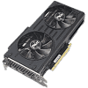
Palit GeForce RTX 3060 Dual OC Review
(6 Comments) »Introduction
Palit introduced its GeForce RTX 3060 Dual OC graphics card today. The RTX 3060 is the most important "Ampere" graphics card for NVIDIA from a volume standpoint, as the xx60 series tends to sell the most to the vast majority of gamers. At a starting price of $329, the RTX 3060 is designed to be a logical upgrade for those still gaming on the GTX 1060 6 GB "Pascal," or even those on the GTX 1660 Ti, bringing them 2nd generation RTX real-time raytracing technology.
The Ampere graphics architecture powering the Palit RTX 3060 Dual OC uses the 2nd generation of RTX technology, combining new Ampere CUDA cores with concurrent FP32+INT32 math performance, 2nd generation RT cores which double the intersection performance over the previous generation, hardware for raytraced motion-blur effects, and 3rd generation Tensor cores that leverage the sparsity phenomenon in neural nets to increase AI inference performance significantly.
The GeForce RTX 3060 is based on the new 8 nm "GA106" silicon, which is making its debut on the desktop platform. The RTX 3060 comes with 3,584 "Ampere" CUDA cores, 112 3rd generation Tensor cores, 28 "Ampere" RT cores, 112 TMUs, and 48 ROPs. NVIDIA has doubled the memory amount over the previous-generation RTX 2060, to 12 GB. The memory bus width and memory type are unchanged—192-bit GDDR6, although the memory clock has been increased slightly to 15 Gbps.
The Palit GeForce RTX 3060 Dual OC is designed for those who just want an RTX 3060 for its gaming performance and features, at pricing as low as possible. It features an innovative dual-fan solution in which most of the airflow from the second fan flows through the heatsink. Palit is giving the card a handy factory-overclock of 1867 MHz (vs. 1777 MHz reference). Palit does not give any guidance on pricing, but we expect the card to be one of the most affordable RTX 3060 models.
| Price | Shader Units | ROPs | Core Clock | Boost Clock | Memory Clock | GPU | Transistors | Memory | |
|---|---|---|---|---|---|---|---|---|---|
| GTX 1060 3 GB | $160 | 1152 | 48 | 1506 MHz | 1708 MHz | 2002 MHz | GP106 | 4400M | 3 GB, GDDR5, 192-bit |
| GTX 1060 | $210 | 1280 | 48 | 1506 MHz | 1708 MHz | 2002 MHz | GP106 | 4400M | 6 GB, GDDR5, 192-bit |
| GTX 1660 | $200 | 1408 | 48 | 1530 MHz | 1785 MHz | 2000 MHz | TU116 | 6600M | 6 GB, GDDR5, 192-bit |
| GTX 1660 Ti | $270 | 1536 | 48 | 1500 MHz | 1770 MHz | 1500 MHz | TU116 | 6600M | 6 GB, GDDR6, 192-bit |
| RTX 2060 | $300 | 1920 | 48 | 1365 MHz | 1680 MHz | 1750 MHz | TU106 | 10800M | 6 GB, GDDR6, 192-bit |
| RX 5700 | $330 | 2304 | 64 | 1465 MHz | 1625 MHz | 1750 MHz | Navi 10 | 10300M | 8 GB, GDDR6, 256-bit |
| GTX 1080 | $330 | 2560 | 64 | 1607 MHz | 1733 MHz | 1251 MHz | GP104 | 7200M | 8 GB, GDDR5X, 256-bit |
| RTX 2060 Super | $380 | 2176 | 64 | 1470 MHz | 1650 MHz | 1750 MHz | TU106 | 10800M | 8 GB, GDDR6, 256-bit |
| RX Vega 64 | $400 | 4096 | 64 | 1247 MHz | 1546 MHz | 953 MHz | Vega 10 | 12500M | 8 GB, HBM2, 2048-bit |
| GTX 1080 Ti | $650 | 3584 | 88 | 1481 MHz | 1582 MHz | 1376 MHz | GP102 | 12000M | 11 GB, GDDR5X, 352-bit |
| RX 5700 XT | $370 | 2560 | 64 | 1605 MHz | 1755 MHz | 1750 MHz | Navi 10 | 10300M | 8 GB, GDDR6, 256-bit |
| RTX 2070 | $340 | 2304 | 64 | 1410 MHz | 1620 MHz | 1750 MHz | TU106 | 10800M | 8 GB, GDDR6, 256-bit |
| RTX 3060 | MSRP: $330 Estimate: $420 | 3584 | 48 | 1320 MHz | 1777 MHz | 1875 MHz | GA106 | 13250M | 12 GB, GDDR6, 192-bit |
| Palit RTX 3060 Dual OC | Estimate: $420 | 3584 | 48 | 1320 MHz | 1867 MHz | 1875 MHz | GA106 | 13250M | 12 GB, GDDR6, 192-bit |
| RTX 2070 Super | $450 | 2560 | 64 | 1605 MHz | 1770 MHz | 1750 MHz | TU104 | 13600M | 8 GB, GDDR6, 256-bit |
| Radeon VII | $680 | 3840 | 64 | 1802 MHz | N/A | 1000 MHz | Vega 20 | 13230M | 16 GB, HBM2, 4096-bit |
| RTX 2080 | $600 | 2944 | 64 | 1515 MHz | 1710 MHz | 1750 MHz | TU104 | 13600M | 8 GB, GDDR6, 256-bit |
| RTX 2080 Super | $690 | 3072 | 64 | 1650 MHz | 1815 MHz | 1940 MHz | TU104 | 13600M | 8 GB, GDDR6, 256-bit |
| RTX 3060 Ti | $700 | 4864 | 80 | 1410 MHz | 1665 MHz | 1750 MHz | GA104 | 17400M | 8 GB, GDDR6, 256-bit |
| RTX 2080 Ti | $1000 | 4352 | 88 | 1350 MHz | 1545 MHz | 1750 MHz | TU102 | 18600M | 11 GB, GDDR6, 352-bit |
| RTX 3070 | $750 | 5888 | 96 | 1500 MHz | 1725 MHz | 1750 MHz | GA104 | 17400M | 8 GB, GDDR6, 256-bit |
| RX 6800 | $850 | 3840 | 96 | 1815 MHz | 2105 MHz | 2000 MHz | Navi 21 | 26800M | 16 GB, GDDR6, 256-bit |
| RX 6800 XT | $1200 | 4608 | 128 | 2015 MHz | 2250 MHz | 2000 MHz | Navi 21 | 26800M | 16 GB, GDDR6, 256-bit |
| RTX 3080 | $1000 | 8704 | 96 | 1440 MHz | 1710 MHz | 1188 MHz | GA102 | 28000M | 10 GB, GDDR6X, 320-bit |
The GeForce Ampere Architecture
Last year, we did a comprehensive article on the NVIDIA GeForce Ampere graphics architecture, along with a deep-dive into the key 2nd Gen RTX technology and various other features NVIDIA is introducing that are relevant to gaming. Be sure to check out that article for more details.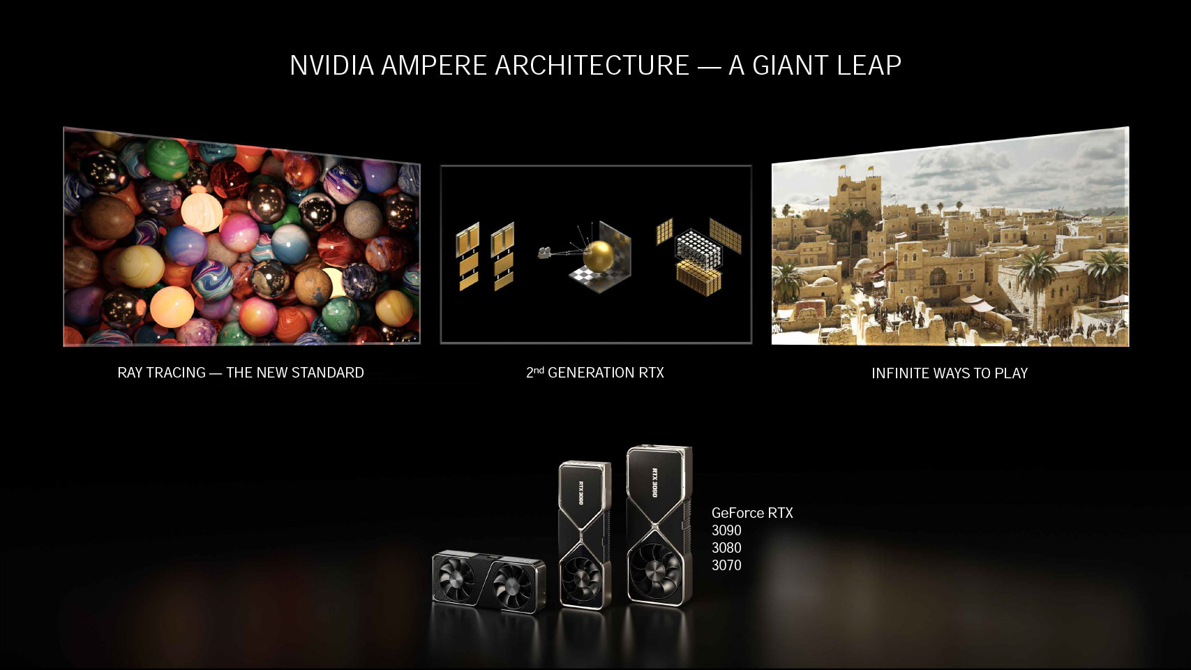
The GeForce Ampere architecture is the first time NVIDIA both converged and diverged its architecture IP between graphics and compute processors. Back in May, NVIDIA debuted Ampere on its A100 Tensor Core compute processor targeted at AI and HPC markets. The A100 Tensor Core is a headless compute chip that lacks all raster graphics components, so NVIDIA could cram in the things relevant to the segment. The GeForce Ampere, however, is a divergence with a redesigned streaming multiprocessor different from that of the A100. These chips have all the raster graphics hardware, display and media acceleration engines, and, most importantly, 2nd generation RT core that accelerates real-time raytracing. A slightly slimmed down version of the 3rd generation tensor core of the A100 also gets carried over. NVIDIA sticks to using GDDR-type memory over expensive memory architectures, such as HBM2E.
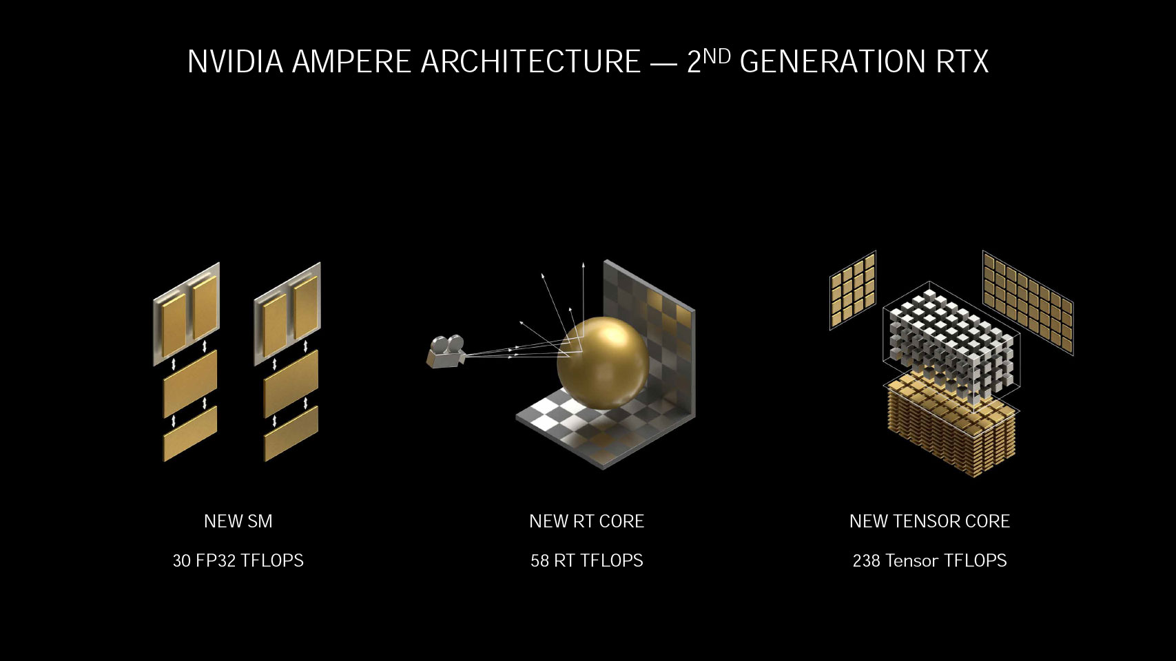
NVIDIA pioneered real-time raytracing on consumer graphics hardware, and three key components make the NVIDIA RTX technology work: the SIMD components, aka CUDA cores, the RT cores, which do the heavy lifting with raytracing, calculating BVH traversal and intersections, and tensor cores, which are hardware components accelerating AI deep-learning neural net building and training. NVIDIA uses an AI-based denoiser for RTX. With Ampere, NVIDIA is introducing new generations of the three components, with the objective being to reduce the performance cost of RTX and nearly double performance over generations. These include the new Ampere streaming multiprocessor that more than doubles FP32 throughput over generations, the 2nd Gen RT core that features hardware that enables new RTX effects, such as raytraced motion blur, and the 3rd generation tensor core, which leverages sparsity in DNNs to increase AI inference performance by an order of magnitude.
GA106 GPU and Ampere SM

The GeForce RTX 3060 debuts NVIDIA's smallest GeForce "Ampere" GPU launched thus far, the "GA106." A successor to the "TU106" from the previous generation, the "GA106" is expected to power the midrange of this generation, with several upcoming SKUs besides the RTX 3060. It's also extensively used in the company's RTX 30-series Mobile graphics family. The "GA106" is built on the same 8 nm silicon fabrication node by Samsung as the rest of the GeForce "Ampere" family. Its die measures 276 mm² and crams in 13.25 billion transistors.
The GA106 silicon features a largely similar component hierarchy to past-generation NVIDIA GPUs, but with the bulk of engineering effort focused on the new Ampere Streaming Multiprocessor (SM). The GPU supports the PCI-Express 4.0 x16 host interface, which doubles the host interface bandwidth over PCI-Express 3.0 x16. NVIDIA has doubled the memory amount over the previous-generation RTX 2060, to 12 GB. The memory bus width is unchanged at 192-bit GDDR6. There's a slight uptick in memory clock, which now runs at 15 Gbps (GDDR6-effective), working out to 360 GB/s memory bandwidth, as opposed to 336 GB/s on the RTX 2060.
The GA106 silicon features three graphics processing clusters (GPCs), the mostly independent subunits of the GPU. Each GPC has five texture processing clusters (TPCs), the indivisible subunit that is the main number-crunching muscle of the GPU. One random TPC is disabled to carve out the RTX 3060. Each TPC shares a PolyMorph engine between two streaming multiprocessors (SMs). The SM is what defines the generation and where the majority of NVIDIA's engineering effort is localized. The Ampere SM crams in 128 CUDA cores, double that of the 64 CUDA cores in the Turing SM. The GeForce RTX 3060 hence ends up with 14 TPCs, 28 streaming multiprocessors, which work out to 3,584 CUDA cores. The chip features 112 Tensor cores, 28 RT cores, 112 TMUs, and 48 ROPs.
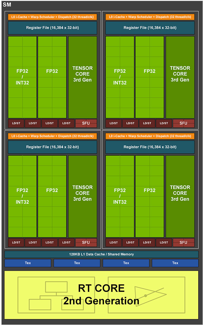

Each GeForce Ampere SM features four processing blocks that each share an L1I cache, warp scheduler, and a register file among 128 CUDA cores. From these, 64 can handle concurrent FP32 and INT32 math operations, while 64 are pure FP32. Each cluster also features a 3rd generation Tensor Core. At the SM level, the four processing blocks share a 128 KB L1D cache that also serves as shared memory; four TMUs and a 2nd generation RT core. As we mentioned, each processing block features two FP32 data paths; one of these consists of CUDA cores that can execute 16 FP32 operations per clock cycle, while the other data path consists of CUDA cores capable of 16 FP32 and 16 INT32 concurrent operations per clock. Each SM also features a tiny, unspecified number of rudimentary FP64 cores, which work at 1/64 the performance of the FP64 cores on the A100 Tensor Core HPC processor. These FP64 cores are only there so double-precision software doesn't run into compatibility problems.
2nd Gen RT Core, 3rd Gen Tensor Core
NVIDIA's 2nd generation RTX real-time raytracing technology sees the introduction of more kinds of raytraced effects. NVIDIA's pioneering technology involves composing traditional raster 3D scenes with certain raytraced elements, such as lighting, shadows, global illumination, and reflections.
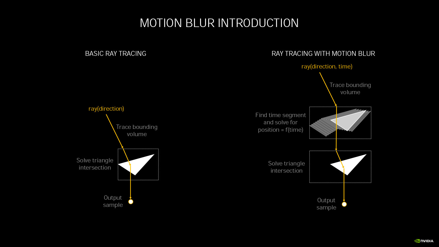
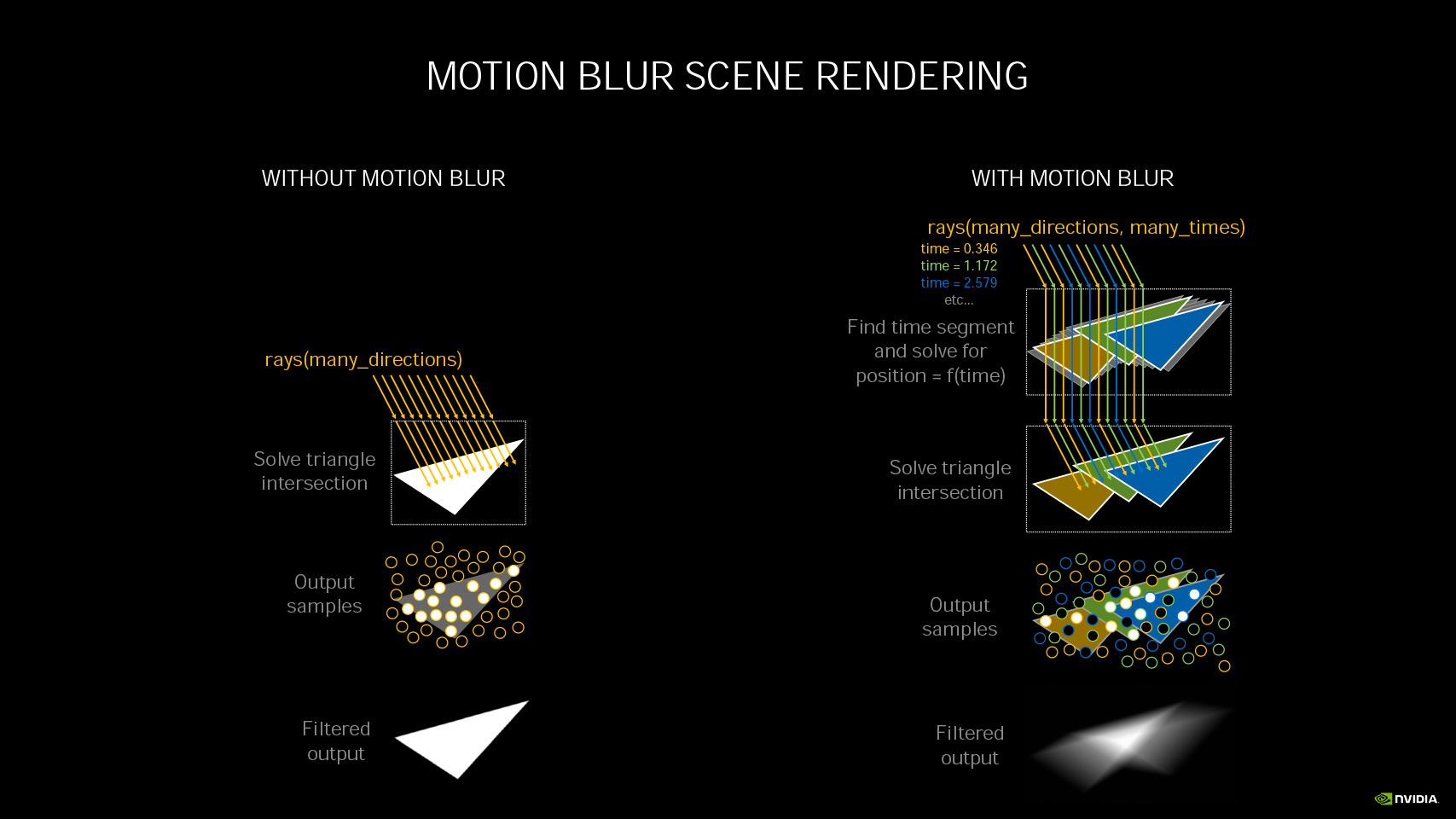
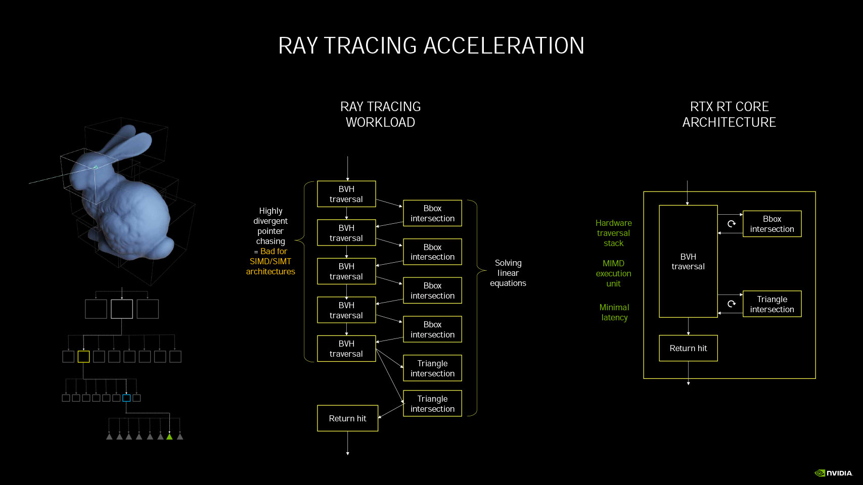
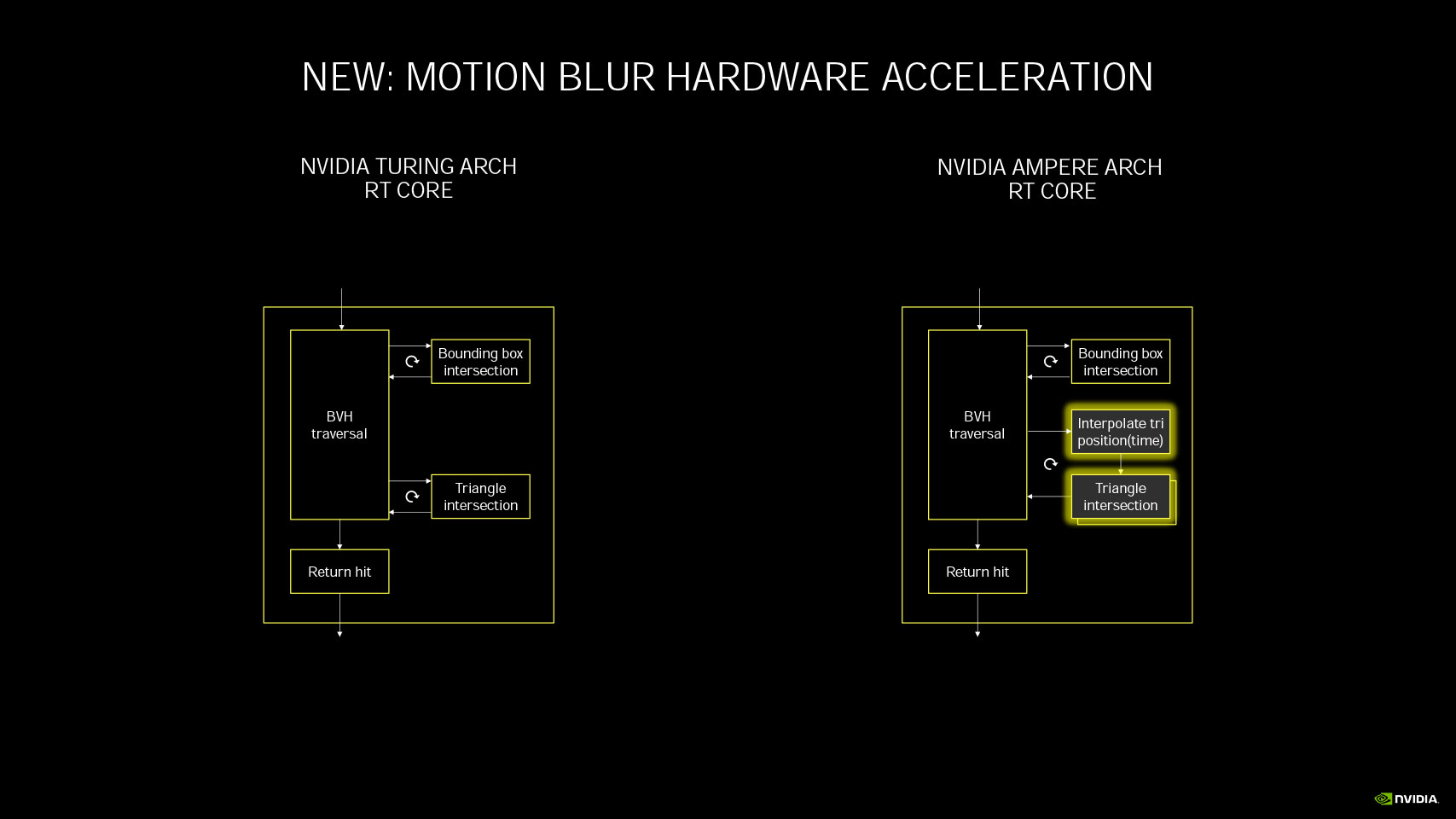
As explained in the Ampere Architecture article, NVIDIA's raytracing philosophy involves heavy bounding volume hierarchy (BVH) traversal, and bounding box/triangle intersection, for which NVIDIA developed a specialized MIMD fixed function in the RT core. Fixed-function hardware handles both the traversal and intersection of rays with bounding boxes or triangles. With the 2nd Gen RT core, NVIDIA is introducing a new component which interpolates triangle position by time. This component enables physically accurate, raytraced motion-blur. Until now, motion-blur was handled as a post-processing effect.
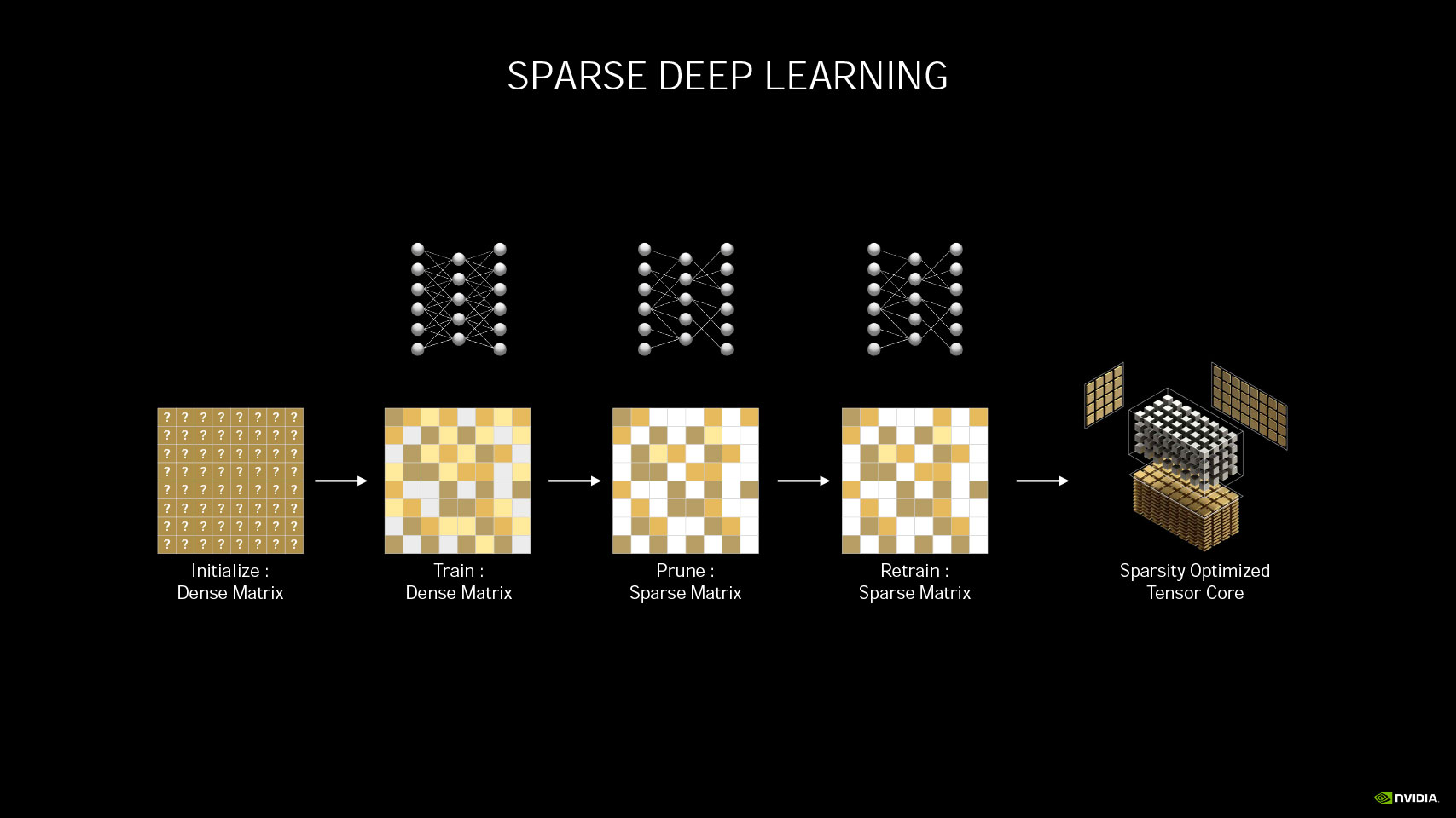
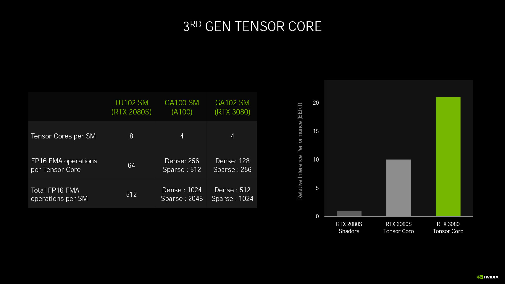
The 3rd generation tensor core sees NVIDIA build on the bulwark of its AI performance leadership, fixed-function hardware designed for tensor math which accelerates AI deep-learning neural-net building and training. AI is heavily leveraged in NVIDIA architectures now as the company uses an AI-based denoiser for its raytracing architecture and to accelerate technologies such as DLSS. Much like the 3rd generation tensor cores on the company's A100 Tensor Core processor that debuted this Spring, the new tensor cores leverage a phenomenon called sparsity—the ability for a DNN to shed its neural net without losing the integrity of its matrix. Think of this like Jenga: You pull pieces from the middle of a column while the column itself stays intact. The use of sparsity increases AI inference performance by an order of magnitude: 256 FP16 FMA operations in a sparse matrix compared to just 64 on the Turing tensor core, and 1024 sparse FP16 FMA ops per SM compared to 512 on the Turing SM, which has double the tensor core counts.
Display and Media
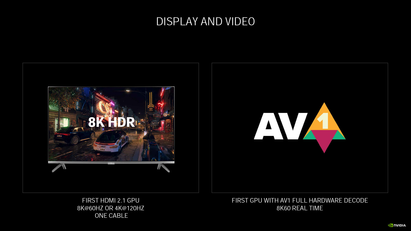
NVIDIA updated the display and media acceleration components of Ampere. To begin with, VirtualLink, or the USB type-C connection, has been removed from the reference design. We've seen no other custom-design cards implement it, so it's safe to assume NVIDIA junked it. The GeForce RTX 3080 puts out three DisplayPort 1.4a, which takes advantage of the new VESA DSC 1.2a compression technology to enable 8K 60 Hz with HDR using a single cable. It also enables 4K at 240 Hz with HDR. The other big development is support for HDMI 2.1, which enables 8K at 60 Hz with HDR, using the same DSC 1.2a codec. NVIDIA claims that DSC 1.2a is "virtually lossless" in quality. Except for the addition of AV1 codec hardware decode, the media acceleration features are largely carried over from Turing. As the next major codec to be deployed by the likes of YouTube and Netflix, AV1 is big. It halves the file size over H.265 HEVC for comparable quality. The new H.266 VVC misses out as the standard was introduced too late into Ampere's development.
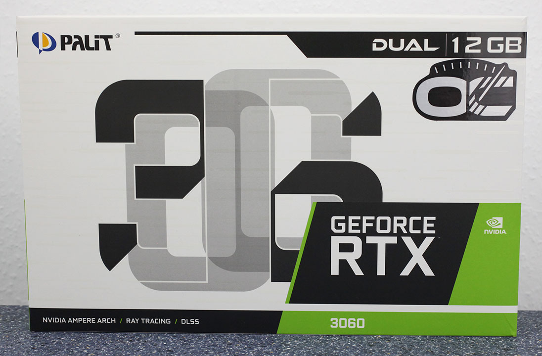
Packaging

Our Patreon Silver Supporters can read articles in single-page format.
Jul 29th, 2025 12:36 CDT
change timezone
Latest GPU Drivers
New Forum Posts
- LCD IPS display (6)
- Looking To Make List Of Keyboard Manufacturers (10)
- Weird issue with Worms: Armageddon on NV GPUs (5)
- 3D Printer Club (570)
- WB actually did it...They closed Monolith. :( (50)
- Upgrade from old x58 system (54)
- 6400c30 vs 8000c36 Ryzen 9800X3D (38)
- PC upgrade after many years (13)
- Gigabyte graphic cards - TIM gel SLIPPAGE problem (169)
- Have you got pie today? (16813)
Popular Reviews
- Herman Miller Logitech G Embody Review - No Pain, No Gain
- Lian Li O11 Dynamic Mini V2 Review
- Lenovo Legion 5i (15IRX10) Review - Feature-Rich and Wallet Friendly
- Upcoming Hardware Launches 2025 (Updated May 2025)
- Noctua NF-A12x25 G2 PWM Fan Review
- Sapphire Radeon RX 9060 XT Pulse OC 16 GB Review - An Excellent Choice
- AQIRYS Sirius Pro Review
- VAXEE XE V2 Wireless Review
- AMD Ryzen 7 9800X3D Review - The Best Gaming Processor
- NVIDIA GeForce RTX 5050 8 GB Review
TPU on YouTube
Controversial News Posts
- AMD's Upcoming UDNA / RDNA 5 GPU Could Feature 96 CUs and 384-bit Memory Bus (134)
- AMD Radeon RX 9070 XT Gains 9% Performance at 1440p with Latest Driver, Beats RTX 5070 Ti (131)
- NVIDIA GeForce RTX 5080 SUPER Could Feature 24 GB Memory, Increased Power Limits (115)
- Intel "Nova Lake-S" Core Ultra 3, Ultra 5, Ultra 7, and Ultra 9 Core Configurations Surface (110)
- DDR6 Memory Arrives in 2027 with 8,800-17,600 MT/s Speeds (99)
- AMD Sampling Next-Gen Ryzen Desktop "Medusa Ridge," Sees Incremental IPC Upgrade, New cIOD (97)
- Intel CEO Confirms SMT To Return to Future CPUs (95)
- NVIDIA Becomes First Company Ever to Hit $4 Trillion Market-Cap (94)