Report an Error
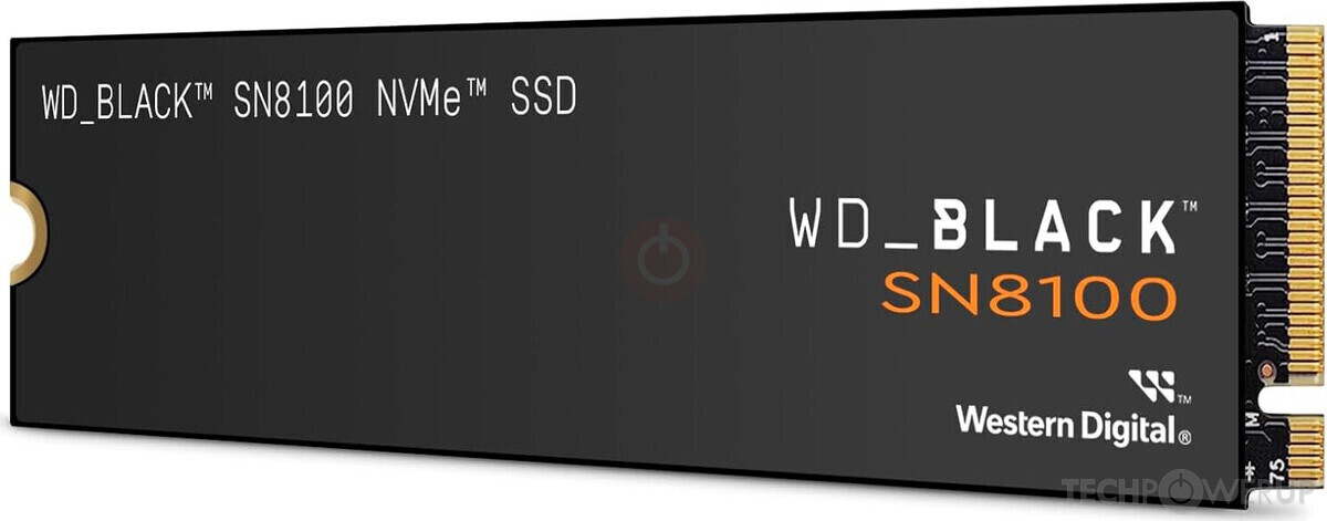
Western Digital SN8100 1 TB
1 TB
Capacity
SM2508
Controller
TLC
Flash
PCIe 5.0 x4
Interface
M.2 2280
Form Factor

Controller

NAND Die
The Western Digital SN8100 is a solid-state drive in the M.2 2280 form factor, launched in May 2025. It is available in capacities ranging from 1 TB to 4 TB. This page reports specifications for the 1 TB variant. With the rest of the system, the Western Digital SN8100 interfaces using a PCI-Express 5.0 x4 connection. The SSD controller is the SM2508 from Silicon Motion, a DRAM cache chip is available. Western Digital has installed 218-layer TLC NAND flash on the SN8100, the flash chips are made by Kioxia. To improve write speeds, a pseudo-SLC cache is used, so bursts of incoming writes are absorbed more quickly. Thanks to support for the fast PCI-Express 5.0 interface, performance is excellent. The SN8100 is rated for sequential read speeds of up to 14,900 MB/s and 11,000 MB/s write; random IO reaches 1600K IOPS for read and 2400K for writes.
The SSD's price at launch is unknown. The warranty length is set to five years, which is an excellent warranty period. Western Digital guarantees an endurance rating of 600 TBW, a typical value for consumer SSDs.
The SSD's price at launch is unknown. The warranty length is set to five years, which is an excellent warranty period. Western Digital guarantees an endurance rating of 600 TBW, a typical value for consumer SSDs.
Solid-State-Drive
| Capacity: | 1 TB (1000 GB) |
|---|---|
| Variants: | 1 TB 2 TB 4 TB |
| Overprovisioning: | 92.7 GB / 10.0 % |
| Production: | Active |
| Released: | May 2025 |
| Part Number: | Unknown |
| Market: | Consumer |
Physical
| Form Factor: | M.2 2280 (Single-Sided) |
|---|---|
| Interface: | PCIe 5.0 x4 |
| Protocol: | NVMe 2.0 |
| Power Draw: |
Unknown (Idle) 7.0 W (Avg) Unknown (Max) |
Controller
| Manufacturer: | Silicon Motion |
|---|---|
| Name: |
SM2508
Find More Drives
|
| Architecture: | ARM 32-bit Cortex-R8 + ARM 32-bit Cortex-M0 |
| Core Count: | 5-Core |
| Frequency: | 1,250 MHz |
| Foundry: | TSMC FinFET |
| Process: | 6 nm |
| Flash Channels: | 8 @ 3,600 MT/s |
| Chip Enables: | 4 |
| Controller Features: | DRAM (enabled) |
NAND Flash
| Manufacturer: | Kioxia |
|---|---|
| Name: | BiCS8 |
| Type: | TLC |
| Technology: | 218-layer |
| Speed: | 3600 MT/s |
| Capacity: | 2 chips @ 4 Tbit |
| Toggle: | 5.1 |
| Topology: | Charge Trap |
| Die Size: | 60 mm² (17.1 Gbit/mm²) |
| Dies per Chip: | 4 dies @ 1 Tbit |
| Planes per Die: | 4 |
| Decks per Die: | 2 |
| Word Lines: |
241 per NAND String
90.5% Vertical Efficiency |
| Read Time (tR): | 40 µs |
| Die Write Speed: | 205 MB/s |
| Endurance: (up to) |
3000 P/E Cycles |
| Page Size: | 16 KB |
| Block Size: | 2748 Pages |
| Plane Size: | 3270 Blocks |
DRAM Cache
| Type: | DDR4 |
|---|---|
| Capacity: |
1024 MB
(1x 1024 MB) |
Performance
| Sequential Read: | 14,900 MB/s |
|---|---|
| Sequential Write: | 11,000 MB/s |
| Random Read: | 1,600,000 IOPS |
| Random Write: | 2,400,000 IOPS |
| Endurance: | 600 TBW |
| Warranty: | 5 Years |
| MTBF: | 1.8 Million Hours |
| Drive Writes Per Day (DWPD): | 0.3 |
| SLC Write Cache: | Yes |
Features
| TRIM: | Yes |
|---|---|
| SMART: | Yes |
| Power Loss Protection: | No |
| Encryption: |
|
| RGB Lighting: | No |
| PS5 Compatible: | Yes |
Notes
Controller:This controller features a Quad-core Cortex-R8 running at 1.25GHz as primary cores, while having a Cortex-M0 as a secondary core for peripheral. NAND Die:This chip is comprised of 8 physical planes (sub planes) with 8KB WLs working as 4 logical planes to keep short BL and WL latency. |
Jul 30th, 2025 06:57 CDT
change timezone
Latest GPU Drivers
New Forum Posts
- 5070ti or 9070xt? (67)
- AMD EXPO Memory issue Suddenly After 7months usage (44)
- AI Job Losses: let's count the losses up, total losses to AI so far 94,000 and counting (81)
- LCD IPS display (13)
- I stop using Windows as my main OS for like 4+ years (12)
- RX6800XT Gigabyte Gaming OC not giving image while being on "OC" switch and even sometimes while being on "silent" switch. (19)
- Slow textures problems and Pop in objects on new system. RTX 5080 (35)
- Samsung 870 EVO - Beware, certain batches prone to failure! (1292)
- AMD Radeon 6900 XT Limited Black Edition Bios Problems - Boost Problems (1)
- What antivirus do you use? (52)
Popular Reviews
- Herman Miller Logitech G Embody Review - No Pain, No Gain
- MSI Claw 8 AI+ A2VM Review
- Lenovo Legion 5i (15IRX10) Review - Feature-Rich and Wallet Friendly
- Lian Li O11 Dynamic Mini V2 Review
- Upcoming Hardware Launches 2025 (Updated May 2025)
- Noctua NF-A12x25 G2 PWM Fan Review
- Sapphire Radeon RX 9060 XT Pulse OC 16 GB Review - An Excellent Choice
- AMD Ryzen 7 9800X3D Review - The Best Gaming Processor
- AQIRYS Sirius Pro Review
- NVIDIA GeForce RTX 5050 8 GB Review
TPU on YouTube
Controversial News Posts
- AMD's Upcoming UDNA / RDNA 5 GPU Could Feature 96 CUs and 384-bit Memory Bus (134)
- AMD Radeon RX 9070 XT Gains 9% Performance at 1440p with Latest Driver, Beats RTX 5070 Ti (131)
- Intel "Nova Lake-S" Core Ultra 3, Ultra 5, Ultra 7, and Ultra 9 Core Configurations Surface (110)
- DDR6 Memory Arrives in 2027 with 8,800-17,600 MT/s Speeds (101)
- AMD Sampling Next-Gen Ryzen Desktop "Medusa Ridge," Sees Incremental IPC Upgrade, New cIOD (97)
- Intel CEO Confirms SMT To Return to Future CPUs (95)
- NVIDIA Becomes First Company Ever to Hit $4 Trillion Market-Cap (94)
- Windows 12 Delayed as Microsoft Prepares Windows 11 25H2 Update (92)