News Posts matching #Cerebras

Return to Keyword Browsing

Cerebras & G42 Break Ground on Condor Galaxy 3 - an 8 exaFLOPs AI Supercomputer

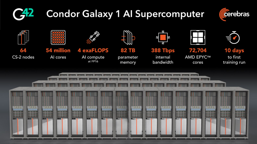
Cerebras Systems, the pioneer in accelerating generative AI, and G42, the Abu Dhabi-based leading technology holding group, today announced the build of Condor Galaxy 3 (CG-3), the third cluster of their constellation of AI supercomputers, the Condor Galaxy. Featuring 64 of Cerebras' newly announced CS-3 systems - all powered by the industry's fastest AI chip, the Wafer-Scale Engine 3 (WSE-3) - Condor Galaxy 3 will deliver 8 exaFLOPs of AI with 58 million AI-optimized cores. The Cerebras and G42 strategic partnership already delivered 8 exaFLOPs of AI supercomputing performance via Condor Galaxy 1 and Condor Galaxy 2, each amongst the largest AI supercomputers in the world. Located in Dallas, Texas, Condor Galaxy 3 brings the current total of the Condor Galaxy network to 16 exaFLOPs.

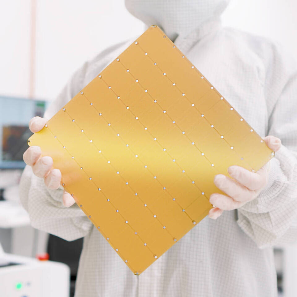
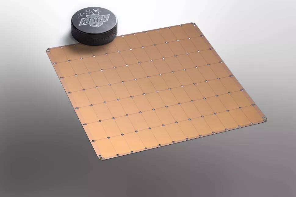
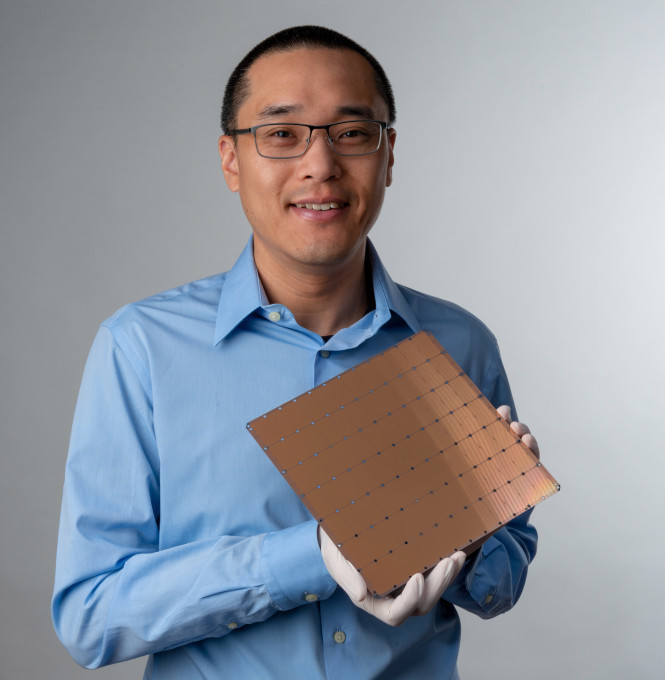
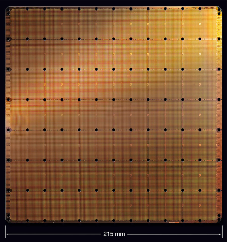
"With Condor Galaxy 3, we continue to achieve our joint vision of transforming the worldwide inventory of AI compute through the development of the world's largest and fastest AI supercomputers," said Kiril Evtimov, Group CTO of G42. "The existing Condor Galaxy network has trained some of the leading open-source models in the industry, with tens of thousands of downloads. By doubling the capacity to 16exaFLOPs, we look forward to seeing the next wave of innovation Condor Galaxy supercomputers can enable." At the heart of Condor Galaxy 3 are 64 Cerebras CS-3 Systems. Each CS-3 is powered by the new 4 trillion transistor, 900,000 AI core WSE-3. Manufactured at TSMC at the 5-nanometer node, the WSE-3 delivers twice the performance at the same power and for the same price as the previous generation part. Purpose built for training the industry's largest AI models, WSE-3 delivers an astounding 125 petaflops of peak AI performance per chip.

Cerebras Systems Unveils World's Fastest AI Chip with 4 Trillion Transistors and 900,000 AI cores

Cerebras Systems, the pioneer in accelerating generative AI, has doubled down on its existing world record of fastest AI chip with the introduction of the Wafer Scale Engine 3. The WSE-3 delivers twice the performance of the previous record-holder, the Cerebras WSE-2, at the same power draw and for the same price. Purpose built for training the industry's largest AI models, the 5 nm-based, 4 trillion transistor WSE-3 powers the Cerebras CS-3 AI supercomputer, delivering 125 petaflops of peak AI performance through 900,000 AI optimized compute cores.

Chinese Researchers Want to Make Wafer-Scale RISC-V Processors with up to 1,600 Cores

According to the report from a journal called Fundamental Research, researchers from the Institute of Computing Technology at the Chinese Academy of Sciences have developed a 256-core multi-chiplet processor called Zhejiang Big Chip, with plans to scale up to 1,600 cores by utilizing an entire wafer. As transistor density gains slow, alternatives like multi-chiplet architectures become crucial for continued performance growth. The Zhejiang chip combines 16 chiplets, each holding 16 RISC-V cores, interconnected via network-on-chip. This design can theoretically expand to 100 chiplets and 1,600 cores on an advanced 2.5D packaging interposer. While multi-chiplet is common today, using the whole wafer for one system would match Cerebras' breakthrough approach. Built on 22 nm process technology, the researchers cite exascale supercomputing as an ideal application for massively parallel multi-chiplet architectures.

Careful software optimization is required to balance workloads across the system hierarchy. Integrating near-memory processing and 3D stacking could further optimize efficiency. The paper explores lithography and packaging limits, proposing hierarchical chiplet systems as a flexible path to future computing scale. While yield and cooling challenges need further work, the 256-core foundation demonstrates the potential of modular designs as an alternative to monolithic integration. China's focus mirrors multiple initiatives from American giants like AMD and Intel for data center CPUs. But national semiconductor ambitions add urgency to prove domestically designed solutions can rival foreign innovation. Although performance details are unclear, the rapid progress shows promise in mastering modular chip integration. Combined with improving domestic nodes like the 7 nm one from SMIC, China could easily create a viable Exascale system in-house.

TSMC Plans to Put a Trillion Transistors on a Single Package by 2030

During the recent IEDM conference, TSMC previewed its process roadmap for delivering next-generation chip packages packing over one trillion transistors by 2030. This aligns with similar long-term visions from Intel. Such enormous transistor counts will come through advanced 3D packaging of multiple chipsets. But TSMC also aims to push monolithic chip complexity higher, ultimately enabling 200 billion transistor designs on a single die. This requires steady enhancement of TSMC's planned N2, N2P, N1.4, and N1 nodes, which are slated to arrive between now and the end of the decade. While multi-chipset architectures are currently gaining favor, TSMC asserts both packaging density and raw transistor density must scale up in tandem. Some perspective on the magnitude of TSMC's goals include NVIDIA's 80 billion transistor GH100 GPU—among today's largest chips, excluding wafer-scale designs from Cerebras.

Yet TSMC's roadmap calls for more than doubling that, first with over 100 billion transistor monolithic designs, then eventually 200 billion. Of course, yields become more challenging as die sizes grow, which is where advanced packaging of smaller chiplets becomes crucial. Multi-chip module offerings like AMD's MI300X and Intel's Ponte Vecchio already integrate dozens of tiles, with PVC having 47 tiles. TSMC envisions this expansion to chip packages housing more than a trillion transistors via its CoWoS, InFO, 3D stacking, and many other technologies. While the scaling cadence has recently slowed, TSMC remains confident in achieving both packaging and process breakthroughs to meet future density demands. The foundry's continuous investment ensures progress in unlocking next-generation semiconductor capabilities. But physics ultimately dictates timelines, no matter how aggressive the roadmap.

Cerebras and G42 Unveil World's Largest Supercomputer for AI Training with 4 ExaFLOPS

Cerebras Systems, the pioneer in accelerating generative AI, and G42, the UAE-based technology holding group, today announced Condor Galaxy, a network of nine interconnected supercomputers, offering a new approach to AI compute that promises to significantly reduce AI model training time. The first AI supercomputer on this network, Condor Galaxy 1 (CG-1), has 4 exaFLOPs and 54 million cores. Cerebras and G42 are planning to deploy two more such supercomputers, CG-2 and CG-3, in the U.S. in early 2024. With a planned capacity of 36 exaFLOPs in total, this unprecedented supercomputing network will revolutionize the advancement of AI globally.

"Collaborating with Cerebras to rapidly deliver the world's fastest AI training supercomputer and laying the foundation for interconnecting a constellation of these supercomputers across the world has been enormously exciting. This partnership brings together Cerebras' extraordinary compute capabilities, together with G42's multi-industry AI expertise. G42 and Cerebras' shared vision is that Condor Galaxy will be used to address society's most pressing challenges across healthcare, energy, climate action and more," said Talal Alkaissi, CEO of G42 Cloud, a subsidiary of G42.

Cerebras Systems Sets Record for Largest AI Models Ever Trained on A Single Device

Cerebras Systems, the pioneer in high performance artificial intelligence (AI) computing, today announced, for the first time ever, the ability to train models with up to 20 billion parameters on a single CS-2 system - a feat not possible on any other single device. By enabling a single CS-2 to train these models, Cerebras reduces the system engineering time necessary to run large natural language processing (NLP) models from months to minutes. It also eliminates one of the most painful aspects of NLP—namely the partitioning of the model across hundreds or thousands of small graphics processing units (GPU).

"In NLP, bigger models are shown to be more accurate. But traditionally, only a very select few companies had the resources and expertise necessary to do the painstaking work of breaking up these large models and spreading them across hundreds or thousands of graphics processing units," said Andrew Feldman, CEO and Co-Founder of Cerebras Systems. "As a result, only very few companies could train large NLP models - it was too expensive, time-consuming and inaccessible for the rest of the industry. Today we are proud to democratize access to GPT-3 1.3B, GPT-J 6B, GPT-3 13B and GPT-NeoX 20B, enabling the entire AI ecosystem to set up large models in minutes and train them on a single CS-2."

Cerebras Updates Wafer Scale Engine on 7 nm - 2.6 Trillion Transistors, 40 GB Onboard SRAM, 850,000 Cores, 12" Wafer

Cerebras has announced the successor to their record-breaking Wafer Scale Engine. The newly re-engineered Wafer Scale Engine 2 has been redesigned for TSMC's 7 nm manufacturing process - a severe improvement over the original's 16 nm. That Cerebras has moved on to TSMC's 7 nm for this giant, wafer-sized accelerator is telling of the confidence and state of yields on TSMC's 7 nm - if the process wasn't considered to be stable and guaranteeing incredibly good yields, I doubt such an effort would have been undertaken.

Hot Chips 2020 Program Announced

Today the Hot Chips program committee officially announced the August conference line-up, posted to hotchips.org. For this first-ever live-streamed Hot Chips Symposium, the program is better than ever!

In a session on deep learning training for data centers, we have a mix of talks from the internet giant Google showcasing their TPUv2 and TPUv3, and a talk from startup Cerebras on their 2nd gen wafer-scale AI solution, as well as ETH Zurich's 4096-core RISC-V based AI chip. And in deep learning inference, we have talks from several of China's biggest AI infrastructure companies: Baidu, Alibaba, and SenseTime. We also have some new startups that will showcase their interesting solutions—LightMatter talking about its optical computing solution, and TensTorrent giving a first-look at its new architecture for AI.
Hot Chips

Cerebras Introduces the CS-1 System, Home to World's First Trillion Transistor Processor

Cerebras has introduced the world to its CS-1 system, which will house the company's (and simultaneously, the industry's) most powerful monolithic accelerator.The CS-1 is an integrated solution the size of 15 industry-standard rack units, and packs everything from the Wafer Scale Engine to cooling systems. The CS-1 consumes 20 kW of power, with a full 4 kW dedicated solely to the cooling subsystem, like fans, pumps, and the heat exchanger, 15 kW dedicated to the chip, and 1 kW is totally lost to power supply inefficiencies. Obviously, power supply modules and other cooling subsystems are redundant, and hot-swappable if need be - you can imagine the computational value lost with each millisecond of downtime that were to occur in such a system.

Cerebras Systems' Wafer Scale Engine is a Trillion Transistor Processor in a 12" Wafer

This news isn't properly today's, but it's relevant and interesting enough that I think warrants a news piece on our page. My reasoning is this: in an era where Multi-Chip Modules (MCM) and a chiplet approach to processor fabrication has become a de-facto standard for improving performance and yields, a trillion-transistor processor that eschews those modular design philosophies is interesting enough to give pause.

The Wafer Scale engine has been developed by Cerebras Systems to face the ongoing increase in demand for AI-training engines. However, in workloads where latency occur a very real impact in training times and a system's capability, Cerebras wanted to design a processor that avoided the need for a communication lane for all its cores to communicate - the system is only limited, basically, by transistors' switching times. Its 400,000 cores communicate seamlessly via interconnects, etched on 42,225 square millimeters of silicon (by comparison, NVIDIA's largest GPU is 56.7 times smaller at "just" 815 square millimeters).
Return to Keyword Browsing
May 21st, 2024 13:04 EDT change timezone

New Forum Posts

Popular Reviews

Controversial News Posts