Wednesday, January 25th 2012

Elpida Memory Develops Resistance RAM Prototype
Elpida Memory, Inc. ("Elpida", TOKYO: 6665 JP), the world's third largest Dynamic Random Access Memory ("DRAM") manufacturer, today announced the development of its first-ever high-speed non-volatile resistance memory (ReRAM) prototype. As the ReRAM prototype was made using a 50-nanometer (nm[1]) process technology it has a memory cell array operation of 64 megabits[2], one of the highest densities possible for ReRAM. The prototype was jointly developed with the New Energy and Industrial Technology Development Organization (NEDO), a Japanese-funded public institution. Further work on ReRAM development is being conducted with Sharp Corporation ("Sharp", TOKYO: 6753 JP), the National Institute of Advanced Industrial Science and Technology (AIST, another Japanese public institution) and the University of Tokyo.
ReRAM (Resistance Random Access Memory) is next-generation semiconductor memory technology that uses material which changes resistance in response to changes in the electric voltage. This new type of non-volatile memory can store data even when the power supply is turned off. Its most attractive feature is that it can read/write data at high speeds using little voltage. While dynamic random-access memory (DRAM) is superior to existing non-volatile memory with respect to read/write speeds and endurance, DRAM quickly loses data when the power supply is removed. NAND flash memory, a leading example of nonvolatile memory, retains data even when the power is removed but has performance measures that are inferior to DRAM.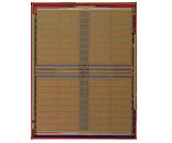 ReRAM, on the other hand, is a type of semiconductor memory that contains the advantages of both DRAM and NAND flash memory. It has a write speed of 10 nanoseconds (ns[3]), about the same as DRAM, and write endurance of more than a million times, or more than 10 times greater than NAND flash.
Elpida plans to continue development toward a 2013 goal of volume production of ReRAM in the gigabit[4] capacity class using a 30nm process technology. If the high-speed durable new memory can be provided at low cost it will contribute enormously to a reduction of memory power consumption. This will make it an attractive storage (recording medium) option in a variety of information technology products, such as smartphones, tablet devices and ultra-thin light notebook PCs.
Elpida continues to develop process migration and other technology related to DRAM and at the same time promotes the development of ReRAM as a promising next-generation memory that can substitute for DRAM functions.1. A nanometer (nm) is one-billionth of a meter.
2. In the case of DRAMs a "megabit" (the symbol for the mega prefix is M) is a unit for expressing an amount of data (volume of information). One gigabit is equal to 1,048,576 bits of data (two raised to the power of 20 or about one million).
3. A nanosecond (ns) is one billionth of a second.
4. In the case of DRAMs a "gigabit" (the symbol for the giga prefix is G) is a unit for expressing an amount of data (volume of information). One gigabit is equal to 1,073,741,824 bits of data (two raised to the power of 30 or about one billion).
ReRAM (Resistance Random Access Memory) is next-generation semiconductor memory technology that uses material which changes resistance in response to changes in the electric voltage. This new type of non-volatile memory can store data even when the power supply is turned off. Its most attractive feature is that it can read/write data at high speeds using little voltage. While dynamic random-access memory (DRAM) is superior to existing non-volatile memory with respect to read/write speeds and endurance, DRAM quickly loses data when the power supply is removed. NAND flash memory, a leading example of nonvolatile memory, retains data even when the power is removed but has performance measures that are inferior to DRAM.

Elpida plans to continue development toward a 2013 goal of volume production of ReRAM in the gigabit[4] capacity class using a 30nm process technology. If the high-speed durable new memory can be provided at low cost it will contribute enormously to a reduction of memory power consumption. This will make it an attractive storage (recording medium) option in a variety of information technology products, such as smartphones, tablet devices and ultra-thin light notebook PCs.
Elpida continues to develop process migration and other technology related to DRAM and at the same time promotes the development of ReRAM as a promising next-generation memory that can substitute for DRAM functions.1. A nanometer (nm) is one-billionth of a meter.
2. In the case of DRAMs a "megabit" (the symbol for the mega prefix is M) is a unit for expressing an amount of data (volume of information). One gigabit is equal to 1,048,576 bits of data (two raised to the power of 20 or about one million).
3. A nanosecond (ns) is one billionth of a second.
4. In the case of DRAMs a "gigabit" (the symbol for the giga prefix is G) is a unit for expressing an amount of data (volume of information). One gigabit is equal to 1,073,741,824 bits of data (two raised to the power of 30 or about one billion).
2 Comments on Elpida Memory Develops Resistance RAM Prototype
But what about Memristor?