Jul 9th, 2025 17:10 CDT
change timezone
Latest GPU Drivers
New Forum Posts
- 5070ti overclock...what are your settings? (46)
- Windows 11 General Discussion (6146)
- Best motherboards for XP gaming (55)
- A Final Fantasy IX Reminiscence - My love letter and homage to one of the best stories ever told (123)
- R-T-B's PNY RTX 5080 OC Photo sideshow. (31)
- Is there a WIFI chip I should get? (0)
- TPU's Nostalgic Hardware Club (20492)
- Do you still use Antivirus software on your latest hardware? (66)
- Rx580 subsystem id (12)
- My first build for graphic design, photo & video editing (45)
Popular Reviews
- NVIDIA GeForce RTX 5050 8 GB Review
- NZXT N9 X870E Review
- Corsair FRAME 5000D RS Review
- Fractal Design Scape Review - Debut Done Right
- Fractal Design Epoch RGB TG Review
- AMD Ryzen 7 9800X3D Review - The Best Gaming Processor
- Sapphire Radeon RX 9060 XT Pulse OC 16 GB Review - An Excellent Choice
- Upcoming Hardware Launches 2025 (Updated May 2025)
- ASUS GeForce RTX 5090 Astral Liquid OC Review - The Most Expensive GPU I've Ever Tested
- Sapphire Radeon RX 9070 XT Nitro+ Review - Beating NVIDIA
TPU on YouTube
Controversial News Posts
- Intel's Core Ultra 7 265K and 265KF CPUs Dip Below $250 (288)
- Some Intel Nova Lake CPUs Rumored to Challenge AMD's 3D V-Cache in Desktop Gaming (140)
- NVIDIA Launches GeForce RTX 5050 for Desktops and Laptops, Starts at $249 (117)
- AMD Radeon RX 9070 XT Gains 9% Performance at 1440p with Latest Driver, Beats RTX 5070 Ti (116)
- NVIDIA GeForce RTX 5080 SUPER Could Feature 24 GB Memory, Increased Power Limits (115)
- Microsoft Partners with AMD for Next-gen Xbox Hardware (105)
- Intel "Nova Lake‑S" Series: Seven SKUs, Up to 52 Cores and 150 W TDP (100)
- NVIDIA DLSS Transformer Cuts VRAM Usage by 20% (97)
Friday, November 24th 2017

Vega 8 Mobile GPU Seemingly Ditches HBM2 Memory, Makes Use of System DDR4 Pool
Update: Industry sources are saying that the 256 MB dedicated system memory to graphics card tasks is currently a firmware limitation, and should be expanded in future firmware revisions to 512 MB and even 1 GB of fully-addressable system DDR4 memory.
AMD's mobile APUs are expected to come with a range of graphics solutions, one of which is the titular Vega 8. Vega 8 isn't supposed to be a high-performance, desktop-class GPU implementation. Instead, it's AMD's counter to NVIDIA's recently announced MX 110 and MX 130 discrete GPUs, which usually deliver relatively low gains (as much as manufacturers want to tout them as extraordinary) when compared to Intel integrated solutions, by far the most widespread IGP. It's expected that Vega 8 performance will slot somewhere around MX110-MX130 levels; and being the low-performance, low cost solution that it's aiming to be, Vega 8 has been made almost unrecognizable from the Vegas we know.
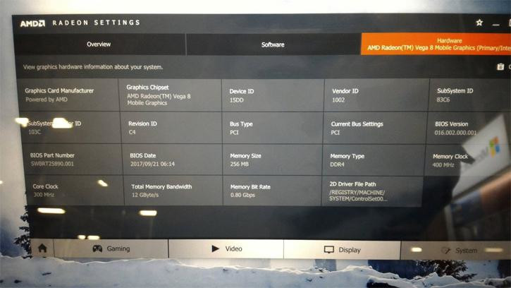
 Vega 8 might signify that the graphics chip has 8 NGCUs at its disposal (Vega 64 has 64, and Vega 56 should be pretty self explanatory), which amounts to just 512 shader units. Via HP's recently outed Envy x360 laptops and a carefully taken photo of the Radeon Settings Hardware panel, we can see that this solution eschews the HBM2 memory (which is only natural, considering the pricing and performance of this solution), and instead, seems to make do with just 256 MB of dedicated system memory - out of a possible 8 GB of DDR4 RAM available in the machine.
The lack of actual dedicated GDDR or HBM memory means that costs are shaved down as much as they can possibly be, but also equates to a performance murder. In terms of shaders, the Vega 8 likely counts 512 (8x64), which is equivalent in number, if not in performance (due to Vega's architecture improvements) to the RX 540. However, the lack of high-speed dedicated memory cuts this graphics solution's available bandwidth down to 12 GB/s - and the core runs at a much cooler and power-sipping 300 MHz base, with up to 1.1 GHz boost clocks.
Sources:
TweakTown, Hardware Info, Thanks @ P4-630!
AMD's mobile APUs are expected to come with a range of graphics solutions, one of which is the titular Vega 8. Vega 8 isn't supposed to be a high-performance, desktop-class GPU implementation. Instead, it's AMD's counter to NVIDIA's recently announced MX 110 and MX 130 discrete GPUs, which usually deliver relatively low gains (as much as manufacturers want to tout them as extraordinary) when compared to Intel integrated solutions, by far the most widespread IGP. It's expected that Vega 8 performance will slot somewhere around MX110-MX130 levels; and being the low-performance, low cost solution that it's aiming to be, Vega 8 has been made almost unrecognizable from the Vegas we know.

The lack of actual dedicated GDDR or HBM memory means that costs are shaved down as much as they can possibly be, but also equates to a performance murder. In terms of shaders, the Vega 8 likely counts 512 (8x64), which is equivalent in number, if not in performance (due to Vega's architecture improvements) to the RX 540. However, the lack of high-speed dedicated memory cuts this graphics solution's available bandwidth down to 12 GB/s - and the core runs at a much cooler and power-sipping 300 MHz base, with up to 1.1 GHz boost clocks.
Jul 9th, 2025 17:10 CDT
change timezone
Latest GPU Drivers
New Forum Posts
- 5070ti overclock...what are your settings? (46)
- Windows 11 General Discussion (6146)
- Best motherboards for XP gaming (55)
- A Final Fantasy IX Reminiscence - My love letter and homage to one of the best stories ever told (123)
- R-T-B's PNY RTX 5080 OC Photo sideshow. (31)
- Is there a WIFI chip I should get? (0)
- TPU's Nostalgic Hardware Club (20492)
- Do you still use Antivirus software on your latest hardware? (66)
- Rx580 subsystem id (12)
- My first build for graphic design, photo & video editing (45)
Popular Reviews
- NVIDIA GeForce RTX 5050 8 GB Review
- NZXT N9 X870E Review
- Corsair FRAME 5000D RS Review
- Fractal Design Scape Review - Debut Done Right
- Fractal Design Epoch RGB TG Review
- AMD Ryzen 7 9800X3D Review - The Best Gaming Processor
- Sapphire Radeon RX 9060 XT Pulse OC 16 GB Review - An Excellent Choice
- Upcoming Hardware Launches 2025 (Updated May 2025)
- ASUS GeForce RTX 5090 Astral Liquid OC Review - The Most Expensive GPU I've Ever Tested
- Sapphire Radeon RX 9070 XT Nitro+ Review - Beating NVIDIA
TPU on YouTube
Controversial News Posts
- Intel's Core Ultra 7 265K and 265KF CPUs Dip Below $250 (288)
- Some Intel Nova Lake CPUs Rumored to Challenge AMD's 3D V-Cache in Desktop Gaming (140)
- NVIDIA Launches GeForce RTX 5050 for Desktops and Laptops, Starts at $249 (117)
- AMD Radeon RX 9070 XT Gains 9% Performance at 1440p with Latest Driver, Beats RTX 5070 Ti (116)
- NVIDIA GeForce RTX 5080 SUPER Could Feature 24 GB Memory, Increased Power Limits (115)
- Microsoft Partners with AMD for Next-gen Xbox Hardware (105)
- Intel "Nova Lake‑S" Series: Seven SKUs, Up to 52 Cores and 150 W TDP (100)
- NVIDIA DLSS Transformer Cuts VRAM Usage by 20% (97)
49 Comments on Vega 8 Mobile GPU Seemingly Ditches HBM2 Memory, Makes Use of System DDR4 Pool
Sucks that they lack dedicated VRAM, Single RAM users can't rejoice.
1) As already mentioned, it's a Raven Ridge iGPU core, so no one expected HBM2 in it.
2) This is a pure speculation:Just from the early "leaked" results R7 2700u was already on par with MX150.
This is not a dGPU. The Ryzen 5 2500U has "Vega 8 graphics", and the screenshots and pictures are of a HP Envy X360 with that specific APU. The announcement of "Ryzen Mobile with Vega Graphics" had not one single mention of HBM. The lack of HBM or dedicated VRAM should thus not be a surprise to anyone.
These are APU graphics with shared memory. APUs do not have dedicated VRAM. Most likely 256MB is a base number, with a variable buffer that adds to this.
This is not news.
DDR4-3200 has 25.6 GB/s
If the Memory-Controller is clever with the same fine-grained DDR4-Handling as the HBCC in the big Vega can.
plus better compression, than the Gap to equal core-count dedicated Cards will shrink.
Edit: of course, the MX150 laptop in question has a lot more thermal/power headroom to boot. I'm looking forward to seeing 25W Ryzen laptops, for sure, both 2500U and 2700U.
hothardware.com/reviews/ryzen-mobile-benchmarks-and-performance-analysis?page=2Who here is talking about that? This is an article concerning pictures of a HP Envy X360 with a Ryzen 5 2500U APU. The Intel+AMD collaboration has nothing to do with this, and is rumored to operate in power envelopes ~5-8 times higher than Ryzen Mobile (65-100W). Also, Intel specifically names that a "discrete graphics chip". I.e. not an iGPU. And it definitely has no relation to Ryzen.
But I've said it from the beginning, Vega is a power hog and using it in laptops is going to be challenging.
Also, we don't know that the Intel+AMD GPU chip is Polaris - they haven't said more than it being a "semi custom design". Might be Vega 11, for all we know. I suppose Polaris could connect to HBM if they designed a chip with an HBM controller - shouldn't be that big of a challenge, if Intel orders enough chips for the silicon redesign to make economic sense.
As for "unreasonable to expect Vega to do the same" - no, not given a suitable SKU. HBM makes very, very little sense in a relatively cheap 15W chip. Remember, the HP laptop in question starts just above $500. If they make a premium 35W-45W version (possibly with a bigger iGPU), that's another story. But HBM is really, really expensive too - there have been estimates that the 8GB dual-stack setup on Vega 56/64 alone (without the interposer) costs ~$150. That's probably more than half of what a 2500U costs for someone like HP.
The APU was physically shown more than 6 months ago. There was no HBM on it then. You could have broken this "news" then. Oh lordy.
If RR had the option for HBM2, AMD would have been shouting it from the rooftops, simply because it would be ridiculously competitive for esports and the like, but still cheap(er than a dGPU), a great sales argument, and a driver for enthusiasm and excitement.
I'm simply arguing to keep assumptions realistic and to base them off of what we know, not what we might hope. And, of course, to not report already-known facts as news.
AMD GPU architectures are modular and you can pretty much mix'n'match any IP blocks.
In case of APUs, they of course use the shared DDR4 memory controller, in case of Vega 10 they use HBCC HBM2 memory controller, in case of Polaris 10 they use GDDR5 memory controller and so on - but they could for example make a Polaris with HBM memory controller (the AMD+Intel chip actually might be Polaris+HBM instead of Vega) or Vega with GDDR memory controller, but that would mean completely new GPU design even when the architecture is the same, and in case of Vega losing certain features since the GDDR memory controllers they have (at least publicly) can't do things the HBCC can
Other sites, Guru3D included, also look amazed by the fact that it doesn't use HBM2. I thought it was common knowledge from about forever. Vega architecture is a GPU architecture, not an HBM2 memory controller. Why would Vega have to be be an HBM2 only solution?
As for performance, let's wait and see some 25W TDP solutions first, judge later. And yes, it does run circles around intel iGPUs, even in this HP laptop.
(sorry if the above isn't too clear, but the significance of Vega not being HBM2-only isn't either)
If I am not mistaken it is rumored for many weeks/months now that AMD will create cheaper cards based on the Vega architecture to replace Polaris models and it was obvious from when those rumors got out, that those cheaper models would not be using HBM2. AMD still tries to create new products by mainly recycling what it already has. Probably one of the reasons Raja left. So people saying that AMD was sticking with HBM2 where right and still are. On an APU design or on a mainstream card, NO ONE expects you to use an expensive solution as HBM2 is. Also, HBM2's main advantage is power consumption and space. On an APU where the integrated GPU doesn't have dedicated memory anyway, why even talk about HBM2? It makes no sense at all.
this is a 15-25w package, hbm alone would make it a 30-40 watt package.
What you're calling "Vega" has several separate IP blocks which can be switched around with different blocks, you could replace the GPU portion with different GPU IP block (for example Polaris-level block), UVD with different version of UVD or ditch the whole UVD for that matter etc etc - and that includes the memory controller as a separate IP block.
Perfect example of this would be Fiji and Tong. They share most of their parts from the same IP level, they're both GCN3 etc etc, but one has HBM and one has GDDR memory controller.
Another example is every single APU they've made - they all share most of their blocks with discrete GPUs but they all use shared DDR memory controller with the CPU, something none of the discrete GPUs has or does.
Similar to this, they could do "Vega" (GCN5) with GDDR memory controller if they so choose, and they've made APU with Vega gfx portion and shared DDR memory controller with the CPU.
There is no "AMD made Vega HBM only", AMD made Vega 10 HBM only, just like they made Fiji HBM only and Tonga GDDR only because there's no sense (or even space) to put two completely different memory controllers in the same chip. They could still do for example Vega 11 with GDDR memory controller or Vega 12 or whatever they want to call such hypothetical chip.