Friday, November 24th 2017

Vega 8 Mobile GPU Seemingly Ditches HBM2 Memory, Makes Use of System DDR4 Pool

Update: Industry sources are saying that the 256 MB dedicated system memory to graphics card tasks is currently a firmware limitation, and should be expanded in future firmware revisions to 512 MB and even 1 GB of fully-addressable system DDR4 memory.

AMD's mobile APUs are expected to come with a range of graphics solutions, one of which is the titular Vega 8. Vega 8 isn't supposed to be a high-performance, desktop-class GPU implementation. Instead, it's AMD's counter to NVIDIA's recently announced MX 110 and MX 130 discrete GPUs, which usually deliver relatively low gains (as much as manufacturers want to tout them as extraordinary) when compared to Intel integrated solutions, by far the most widespread IGP. It's expected that Vega 8 performance will slot somewhere around MX110-MX130 levels; and being the low-performance, low cost solution that it's aiming to be, Vega 8 has been made almost unrecognizable from the Vegas we know.
Vega 8 might signify that the graphics chip has 8 NGCUs at its disposal (Vega 64 has 64, and Vega 56 should be pretty self explanatory), which amounts to just 512 shader units. Via HP's recently outed Envy x360 laptops and a carefully taken photo of the Radeon Settings Hardware panel, we can see that this solution eschews the HBM2 memory (which is only natural, considering the pricing and performance of this solution), and instead, seems to make do with just 256 MB of dedicated system memory - out of a possible 8 GB of DDR4 RAM available in the machine.

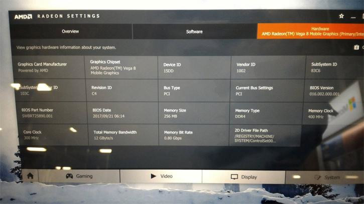
The lack of actual dedicated GDDR or HBM memory means that costs are shaved down as much as they can possibly be, but also equates to a performance murder. In terms of shaders, the Vega 8 likely counts 512 (8x64), which is equivalent in number, if not in performance (due to Vega's architecture improvements) to the RX 540. However, the lack of high-speed dedicated memory cuts this graphics solution's available bandwidth down to 12 GB/s - and the core runs at a much cooler and power-sipping 300 MHz base, with up to 1.1 GHz boost clocks.
Sources: TweakTown, Hardware Info, Thanks @ P4-630!
Add your own comment

49 Comments on Vega 8 Mobile GPU Seemingly Ditches HBM2 Memory, Makes Use of System DDR4 Pool

#26
bug
KaotikSigh, the "GPU" portion doesn't really care if they stick a HBCC HBM memory controller or some other memory controller in there.
What you're calling "Vega" has several separate IP blocks which can be switched around with different blocks, you could replace the GPU portion with different GPU IP block (for example Polaris-level block), UVD with different version of UVD or ditch the whole UVD for that matter etc etc - and that includes the memory controller as a separate IP block.

Perfect example of this would be Fiji and Tong. They share most of their parts from the same IP level, they're both GCN3 etc etc, but one has HBM and one has GDDR memory controller.
Another example is every single APU they've made - they all share most of their blocks with discrete GPUs but they all use shared DDR memory controller with the CPU, something none of the discrete GPUs has or does.

Similar to this, they could do "Vega" (GCN5) with GDDR memory controller if they so choose, and they've made APU with Vega gfx portion and shared DDR memory controller with the CPU.

There is no "AMD made Vega HBM only", AMD made Vega 10 HBM only, just like they made Fiji HBM only and Tonga GDDR only because there's no sense (or even space) to put two completely different memory controllers in the same chip. They could still do for example Vega 11 with GDDR memory controller or Vega 12 or whatever they want to call such hypothetical chip.
Yes, and? If it's modular it doesn't cost extra to replace the memory controller? We all know the memory controller is a separate block, it's not like it's built into the shares or something. That was not the point.
Posted on Reply
#27
Kanan
Tech Enthusiast & Gamer
12GB/s bandwidth means it is running atrocious single channel DDR4 and low DDR4 clocks as well. It can have easily over 40 GB/s with proper dual channel / high clocked DDR4. Some of the APU's I built have 38,4 GB/s with DDR3 2400. That's kinda the minimum speed you want to have with those, it's equivalent to dual channel DDR4 2400 - needless to say you can go far higher than that.
Posted on Reply
#28
Kaotik
bugYes, and? If it's modular it doesn't cost extra to replace the memory controller? We all know the memory controller is a separate block, it's not like it's built into the shares or something. That was not the point.
Of course designing each GPU adds costs, point was that AMD didn't design "Vega HBM only" or "This shows Vega can use other than HBM" like was claimed here

late edit: fixed terrible typos
Posted on Reply
#29
Shamalamadingdong
bugYes, and? If it's modular it doesn't cost extra to replace the memory controller? We all know the memory controller is a separate block, it's not like it's built into the shares or something. That was not the point.
Well, it kinda does cost extra.

You need to make changes to the die meaning you need to make a new mask for the Fab and then it needs to tape-out and you need to validate it. It'll take many months and millions to get such a product ready. It's not as simple as switching a component on an assembly line. It becomes a new chip.

If the memory controller was external, then it should be really simple. But it is true that they don't need to start from scratch to implement GDDR on Vega. The blocks are interchangeable with little work.

Integrated graphics are designed with system memory in mind and always have been for AMD. That's why it's a surprise to no one that Raven Ridge does not have HBM. It's been known for months. The package would also be much different to support dedicated memory and would add considerable cost, size, complexity and power. You'd probably see a $100-200 premium (conservative estimate) on every single device with a Raven Ridge chip (depending on memory configuration). Alternatively they would have to spend those millions and months making two chips. There is a budget constraint going on at AMD. It simply isn't feasible to do so. They need to make one-size-fits-all chips to get as much money out of each chip and so far it's working but it isn't the best for every situation. Hopefully, AMD can start making multiple chips per generation like Intel and Nvidia does; perhaps next year.
Posted on Reply
#30
medi01
Note how ironically inadequate OP tone is:

3DMark 11 scores for the Vega 8 in the HP convertible are unequivocally faster than the common HD Graphics solutions found on the Intel U-class family. They may not be as impressive as the recently leaked graphics capabilities of the rumored AMD-Intel Core i7-8705G, but performance is still comfortably midway between the Maxwell GeForce 940MX and Pascal GeForce MX150. When considering that these Nvidia alternatives are discrete GPUs, we can't help but commend AMD's powerful integrated solution.

www.notebookcheck.net/Our-first-Ryzen-5-2500U-benchmarks-are-in-and-Intel-has-every-reason-to-worry.266618.0.html
bugI can't wait to see what they have to say about this.
I only have to say /facepalm.
And it isn't even the fastest APU.
Posted on Reply
#31
Apocalypsee
AquinusThere is plenty of room in most towers to use off-package DRAM. HBM should be used for mobile platforms where space and power are at a premium. Even for low end hardware, just use less of it. Even one stack of HBM2 could do wonders for performance on a mixed GPU/CPU package. I would expect it to essentially behave like Crystalwell did on eDRAM-enabled Intel CPUs except with more capacity and performance.
This is what I thinking is optimal for APU initially, but the complexity of interposer and HBM requires additional circuitry and power planes going to complicate matters especially on mobile because lets face it, it still going to require regular DDR memory to operate.

What AMD should done is like what they planned on Kaveri by implementing quad channel memory (256-bit) and/or GDDR5 memory. You can read Anandtech article about it. IMO for mobile they could just ditch regular DDR and use GDDR5. There's no need for additional slot just soldered it on the motherboard. GDDR5 have been around since 2007, it shoudnt costs that much. A standard dual channel (128-bit) GDDR5 runs at measly 1GHz (4GHz effective) netted 64GB/s bandwidth. Modern GDDR5 runs at twice the speed of that.
Posted on Reply
#32
Aquinus
Resident Wat-man
ApocalypseeThis is what I thinking is optimal for APU, but the complexity of interposer and HBM requires additional circuitry and power planes going to complicate matters especially on mobile because lets face it, it still going to require regular DDR memory to operate.
Not if you cut out a memory channel. If HBM is treated like another layer of cache, they could reduce the size of the DDR4 controller to make room and free up power to be used by HBM. Also, just one stack of HBM means less power as well compared to two. This really isn't any different from how L2 and L3 cache work or how Crystalwell works. There are times when you need fast memory access and there are times when you need bulk memory access and adding a layer between external system memory and cache opens the possibility where more memory helps so you don't have to swap to disk but, there isn't necessarily a requirement for external DRAM to be present. To me, that makes a lot more sense because you're retaining the benefits of both without going 100% in either direction. Something like this would intrigue me for a HTPC or a small form-factor workstation.
Posted on Reply
#33
Apocalypsee
AquinusNot if you cut out a memory channel. If HBM is treated like another layer of cache, they could reduce the size of the DDR4 controller to make room and free up power to be used by HBM. Also, just one stack of HBM means less power as well compared to two. This really isn't any different from how L2 and L3 cache work or how Crystalwell works. There are times when you need fast memory access and there are times when you need bulk memory access and adding a layer between external system memory and cache opens the possibility where more memory helps so you don't have to swap to disk but, there isn't necessarily a requirement for external DRAM to be present. To me, that makes a lot more sense because you're retaining the benefits of both without going 100% in either direction. Something like this would intrigue me for a HTPC or a small form-factor workstation.
Implementing HBM is not as easy as eDRAM. Even though its a single stack it still requires interposer and other circuitry involving with it. I dont believe it could be implemented on the same socket unlike Intel did on Broadwell (except that Intel did the 'new motherboard for new CPU' thing they always did). AMD could not afford to do this, since both Fury and Vega desktop doesnt do well and it will jack up the price significantly for what its aimed for.
Posted on Reply
#34
Imsochobo
AquinusNot if you cut out a memory channel. If HBM is treated like another layer of cache, they could reduce the size of the DDR4 controller to make room and free up power to be used by HBM. Also, just one stack of HBM means less power as well compared to two. This really isn't any different from how L2 and L3 cache work or how Crystalwell works. There are times when you need fast memory access and there are times when you need bulk memory access and adding a layer between external system memory and cache opens the possibility where more memory helps so you don't have to swap to disk but, there isn't necessarily a requirement for external DRAM to be present. To me, that makes a lot more sense because you're retaining the benefits of both without going 100% in either direction. Something like this would intrigue me for a HTPC or a small form-factor workstation.
Disclaimer: This comment isn't all directely meant for the quoted person only the top is, rest is just in general.

The fact is that the APU doesn't have a memory controller most likely, it uses the CPU memory controller.
in APU's you can do that.

--

They are using 15W fucking watts.
Know how much power a GTX1080 use? take just the memory and you have a complete laptop running and playing a game at less power than the memory on a 1080.
So, Should we go back to the 10 cm thick ultrabook laptops cause we as desktop gamers find something 2x the speed of intel igpu is bad for ultraportable laptops that use 15-25 watts?
This whole thread contains a few smart guys who understand the product and everyone else that thinks this is meant to destroy Nvidia dedicated gpu's... Nope.
If amd makes a 45 W part with memory then we can see what they can do.

This is 110% made to fight Intel-intel systems and if they can fix video playback power consumption I really think they nailed it... they beat Intel then
Posted on Reply
#35
Aquinus
Resident Wat-man
ApocalypseeImplementing HBM is not as easy as eDRAM. Even though its a single stack it still requires interposer and other circuitry involving with it. I dont believe it could be implemented on the same socket unlike Intel did on Broadwell (except that Intel did the 'new motherboard for new CPU' thing they always did). AMD could not afford to do this, since both Fury and Vega desktop doesnt do well and it will jack up the price significantly for what its aimed for.
You're right. Something like this doesn't happen overnight but when you scale up production, these costly things become less costly over time. My point is that it's doable and could be a possible middle ground that could scale from the small to the big but, a change like that takes time and money.
Posted on Reply
#36
Kaotik
AquinusYou're right. Something like this doesn't happen overnight but when you scale up production, these costly things become less costly over time. My point is that it's doable and could be a possible middle ground that could scale from the small to the big but, a change like that takes time and money.
It would require completely new chip layout from the scratch, that's a multimillion project and with AMDs limited R&D budget you need to take your picks on what you want. For what it's worth, they apparently are bringing a "real HPC APU" which will just go leaps and bounds beyond anything out there, including the AMD+Intel-chip with up to 16 Zen-cores and around 4 TF Vega-based GPU + 2 HBM stacks on MCM module, if the very old plans weren't scratched that is.
Posted on Reply
#37
Kanan
Tech Enthusiast & Gamer
ShamalamadingdongWell, it kinda does cost extra.

You need to make changes to the die meaning you need to make a new mask for the Fab and then it needs to tape-out and you need to validate it. It'll take many months and millions to get such a product ready. It's not as simple as switching a component on an assembly line. It becomes a new chip.

If the memory controller was external, then it should be really simple. But it is true that they don't need to start from scratch to implement GDDR on Vega. The blocks are interchangeable with little work.

Integrated graphics are designed with system memory in mind and always have been for AMD. That's why it's a surprise to no one that Raven Ridge does not have HBM. It's been known for months. The package would also be much different to support dedicated memory and would add considerable cost, size, complexity and power. You'd probably see a $100-200 premium (conservative estimate) on every single device with a Raven Ridge chip (depending on memory configuration). Alternatively they would have to spend those millions and months making two chips. There is a budget constraint going on at AMD. It simply isn't feasible to do so. They need to make one-size-fits-all chips to get as much money out of each chip and so far it's working but it isn't the best for every situation. Hopefully, AMD can start making multiple chips per generation like Intel and Nvidia does; perhaps next year.
Well at least Intel is doing it for and with AMD, also making it possible by their own superior "interposer" (which isn't called Interposer but I forgot the name).
ApocalypseeWhat AMD should done is like what they planned on Kaveri by implementing quad channel memory (256-bit) and/or GDDR5 memory. You can read Anandtech article about it. IMO for mobile they could just ditch regular DDR and use GDDR5. There's no need for additional slot just soldered it on the motherboard. GDDR5 have been around since 2007, it shoudnt costs that much. A standard dual channel (128-bit) GDDR5 runs at measly 1GHz (4GHz effective) netted 64GB/s bandwidth. Modern GDDR5 runs at twice the speed of that.
GDDR5 has extremely bad latencies compared to DDR3/4 and is not really suitable for normal PC usage. If it'd be they would've already done that long long ago.

HBM2 for any APU would be possible, but only with Intel's superior "interposer" tech, because that one is far easier and cheaper to produce. But I don't think Intel is giving it to AMD just like that - just for the one project they are working on in tandem.
Posted on Reply
#38
Valantar
john_Don't shoot the messenger :p

Other sites, Guru3D included, also look amazed by the fact that it doesn't use HBM2.
Now, I don't read Guru3D frequently, but when I've stumbled across that site from time to time it hasn't struck me as the highest-quality reporting in town, to put it mildly. Of course better than Videocardz and WCCFTech, but that's about it.
AquinusYou're right. Something like this doesn't happen overnight but when you scale up production, these costly things become less costly over time. My point is that it's doable and could be a possible middle ground that could scale from the small to the big but, a change like that takes time and money.
HBM2 supply is still very meagre, and both HBM and implementing it would be crazy expensive. Estimates for Vega say its dual 4GB stacks cost ~$150 before the cost of the interposer and all that jazz. In other words, a single 4GB stack would be $75, and the interposer and thus complicated mounting would be at least another $25, giving us a neat price hike of >$100 for a normally ~$200 APU (possibly a bit more, but Intel's competing solutions list at $303, so definitely less than that). Does that seem like a good idea to you? Even if halving the memory amount brought that down to ~$65, that's still way too much. And there's no indication HBM or interposers will become significantly cheaper over the next year.


Now for some speculation: could AMDs collaboration with Intel have given them access to EMIB on AMD-only products? That would be a pretty reasonable thing to licence, no? If so, that would bode for some production cost drops in GPUs, and possibly APUs with HBM down the line.
Posted on Reply
#39
john_
EMIB might be nice for future discrete GPUs, but probably interposer is good enough for that job. EMIB in laptops with Ryzen CPUs or even APUs, don't know if it makes sense, considering that AMD would have to be able to persuade OEMs to create enough models with AMD CPUs/APUs to justify any payment to Intel, to use that tech. I doubt intel gives any kind of access/license to AMD for the EMIB. They did collaborated closely in the creation of the Kaby lake G, but I think, in this case, things are as simple as "intel is a customer of AMD" and nothing more, for now. Intel gone to AMD and said "We want one of your GPUs to put next to a Kaby lake using this tech. You can help us do it, or we can go to Nvidia, even if we hate the idea".
Posted on Reply
#40
Aquinus
Resident Wat-man
ValantarHBM2 supply is still very meagre, and both HBM and implementing it would be crazy expensive. Estimates for Vega say its dual 4GB stacks cost ~$150 before the cost of the interposer and all that jazz. In other words, a single 4GB stack would be $75, and the interposer and thus complicated mounting would be at least another $25, giving us a neat price hike of >$100 for a normally ~$200 APU (possibly a bit more, but Intel's competing solutions list at $303, so definitely less than that). Does that seem like a good idea to you? Even if halving the memory amount brought that down to ~$65, that's still way too much. And there's no indication HBM or interposers will become significantly cheaper over the next year.
Tooling and scaling production tends to reduce the cost of manufacturing complex hardware like HBM. What I said prior is 100% applicable:
AquinusSomething like this doesn't happen overnight but when you scale up production, these costly things become less costly over time. My point is that it's doable and could be a possible middle ground that could scale from the small to the big but, a change like that takes time and money.
Let me put it another way: It won't cost that much forever.
Posted on Reply
#41
Valantar
john_EMIB might be nice for future discrete GPUs, but probably interposer is good enough for that job. EMIB in laptops with Ryzen CPUs or even APUs, don't know if it makes sense, considering that AMD would have to be able to persuade OEMs to create enough models with AMD CPUs/APUs to justify any payment to Intel, to use that tech. I doubt intel gives any kind of access/license to AMD for the EMIB. They did collaborated closely in the creation of the Kaby lake G, but I think, in this case, things are as simple as "intel is a customer of AMD" and nothing more, for now. Intel gone to AMD and said "We want one of your GPUs to put next to a Kaby lake using this tech. You can help us do it, or we can go to Nvidia, even if we hate the idea".
Isn't the whole point of EMIB that it's far cheaper, mechanically simpler and easier to implement than an interposer? Saying that an interposer "is probably good enough" misses the point entirely when the point of EMIB is to do the same for less, not more or better. This is also why I think AMD licensing EMIB makes sense, as it (given a reasonable licensing deal, which KBL-G might give them) would significantly cut production costs for their high-end GPUs, as well as open up the possibility of using HBM on lower end products where the added interposer cost would be too steep. While there's no doubt AMD is getting paid for their GPUs in KBL-G, it seems odd to me that they'd agree to something like that without some exchange of technology or licensing baked into it.
AquinusTooling and scaling production tends to reduce the cost of manufacturing complex hardware like HBM. What I said prior is 100% applicable:

Let me put it another way: It won't cost that much forever.
While that is true, this is still not the time to implement HBM with an interposer in a relatively cheap mobile APU. AMD has no control over HBM production, and supply is short and will continue to be so for a while yet (unless HBM production somehow is entirely immune to the current DRAM/NAND production shortages - which doesn't make sense). I'd be shocked to see HBM hit a mid-range APU before it hits midrange GPUs - margins are far higher there, after all. And for now, HBM is for the high end. Sure, Intel is putting it in KBL-G, but Intel has cash to throw around, and entirely owns the market for high-end mobile devices. They're in a far better place to do so. A generation or two from now, the situation will probably be different.
Posted on Reply
#42
Shamalamadingdong
ValantarIsn't the whole point of EMIB that it's far cheaper, mechanically simpler and easier to implement than an interposer? Saying that an interposer "is probably good enough" misses the point entirely when the point of EMIB is to do the same for less, not more or better. This is also why I think AMD licensing EMIB makes sense, as it (given a reasonable licensing deal, which KBL-G might give them) would significantly cut production costs for their high-end GPUs, as well as open up the possibility of using HBM on lower end products where the added interposer cost would be too steep. While there's no doubt AMD is getting paid for their GPUs in KBL-G, it seems odd to me that they'd agree to something like that without some exchange of technology or licensing baked into it.

While that is true, this is still not the time to implement HBM with an interposer in a relatively cheap mobile APU. AMD has no control over HBM production, and supply is short and will continue to be so for a while yet (unless HBM production somehow is entirely immune to the current DRAM/NAND production shortages - which doesn't make sense). I'd be shocked to see HBM hit a mid-range APU before it hits midrange GPUs - margins are far higher there, after all. And for now, HBM is for the high end. Sure, Intel is putting it in KBL-G, but Intel has cash to throw around, and entirely owns the market for high-end mobile devices. They're in a far better place to do so. A generation or two from now, the situation will probably be different.
Don't expect EMIB to be nothing but Intel exclusive unless Intel finds issues capitalizing on it and it suddenly makes sense to open it up for licensing. EMIB is a definite ace for Intel. It opens a lot of new avenues (including KBL-G) but allowing the competition to even the playing field and eventually making better products would be a bad move and Intel doesn't need the money that badly - it's the other way around. AMD probably can't afford what Intel would require to relinquish the exclusivity. We already see a lot of what AMD's doing falling flat because they lack resources. Of course the counter-argument would be that they need to spend money to earn money but there are simply limits to what they can do because every move they make could end up tipping the scales towards bankruptcy.
Posted on Reply
#43
Valantar
ShamalamadingdongDon't expect EMIB to be nothing but Intel exclusive unless Intel finds issues capitalizing on it and it suddenly makes sense to open it up for licensing. EMIB is a definite ace for Intel. It opens a lot of new avenues (including KBL-G) but allowing the competition to even the playing field and eventually making better products would be a bad move and Intel doesn't need the money that badly - it's the other way around. AMD probably can't afford what Intel would require to relinquish the exclusivity. We already see a lot of what AMD's doing falling flat because they lack resources. Of course the counter-argument would be that they need to spend money to earn money but there are simply limits to what they can do because every move they make could end up tipping the scales towards bankruptcy.
You're not wrong, but what does AMD have that Intel needs? GPU tech, or more specifically GPU patents. There's no way Intel will be able to develop their own dGPU - even with the help of Raja Koduri - without stepping on the toes of AMD or Nvidia, so they rather desperately need a patent licencing agreement. The one they had in place with Nvidia expired (even if it still gives them access to patents from before its expiration), so AMD is a natural business partner there. And as the one holding all the rights to EMIB, Intel could essentially tailor a licence that would make sure AMD didn't use the tech in any products that compete with Intel's bread and butter, such as server hardware and the like. An agreement like this could make licencing AMD's GPU patents a heck of a lot cheaper for Intel, that's for sure. And even if Intel has the cash, corporations generally don't like giving away cash when they can avoid it.
Posted on Reply
#44
Shamalamadingdong
ValantarYou're not wrong, but what does AMD have that Intel needs? GPU tech, or more specifically GPU patents. There's no way Intel will be able to develop their own dGPU - even with the help of Raja Koduri - without stepping on the toes of AMD or Nvidia, so they rather desperately need a patent licencing agreement. The one they had in place with Nvidia expired (even if it still gives them access to patents from before its expiration), so AMD is a natural business partner there. And as the one holding all the rights to EMIB, Intel could essentially tailor a licence that would make sure AMD didn't use the tech in any products that compete with Intel's bread and butter, such as server hardware and the like. An agreement like this could make licencing AMD's GPU patents a heck of a lot cheaper for Intel, that's for sure. And even if Intel has the cash, corporations generally don't like giving away cash when they can avoid it.
Intel could do like Apple and attempt to make their GPU tech a giant black box and hope their competitors don't find any evidence to support patent litigation or hope that competitors are afraid of opening up Pandora's box which in this case consists of large scale patent warfare.

But let's assume Intel trades EMIB for either general GPU patents or Radeon tech. Is it of equal value? I don't think so personally.
And who's to say AMD isn't working on something similar to EMIB (of course without infringing)? It would seem wise to have had something in the works to replace interposers unless AMD has had no foresight as to the money drain HBM and interposers have turned out to be.

I have no doubt AMD wants EMIB or an EMIB-like solution if nothing else but to save money. Intel doesn't like to play ball though; they only do when they absolutely have to.
Examples being opening up Thunderbolt, KBL-G, relationship with Microsoft and Apple (although funnily enough only on Mac; they told Apple to fuck off when they asked Intel to develop a processor for phones and look how much they regret that today as it wasn't the money sink they thought it'd be).
Other than that, Intel have a habit of making sure the competition has a hard time to put it mildly.

Don't get me wrong, I want AMD to be able to execute on their strategy which ultimately relies on tech enabling the connection of chips together and EMIB is a revolutionary way to do that.
Posted on Reply
#45
john_
ValantarIsn't the whole point of EMIB that it's far cheaper, mechanically simpler and easier to implement than an interposer? Saying that an interposer "is probably good enough" misses the point entirely when the point of EMIB is to do the same for less, not more or better. This is also why I think AMD licensing EMIB makes sense, as it (given a reasonable licensing deal, which KBL-G might give them) would significantly cut production costs for their high-end GPUs, as well as open up the possibility of using HBM on lower end products where the added interposer cost would be too steep. While there's no doubt AMD is getting paid for their GPUs in KBL-G, it seems odd to me that they'd agree to something like that without some exchange of technology or licensing baked into it.
If I am not mistaken, interposer is AMD's patent. So, maybe it makes more sense AMD to improve the interposer, than trying to come to an agreement with intel. Especially if the difference in costs and complexity are not significant(you say far cheaper, could be, any links?). Also, while it makes perfect sense to prefer EMIB in a very slim laptop, if AMD is not going to create something like an APU with a very strong GPU and HBM or HBM2 sitting next to that APU, for ultra slim devices, there isn't really any important reason to go and beg intel. On discrete GPUs, having the main chip one or two millimeters higher than the PCB, isn't really a problem.
Posted on Reply
#46
Valantar
john_If I am not mistaken, interposer is AMD's patent. So, maybe it makes more sense AMD to improve the interposer, than trying to come to an agreement with intel. Especially if the difference in costs and complexity are not significant(you say far cheaper, could be, any links?). Also, while it makes perfect sense to prefer EMIB in a very slim laptop, if AMD is not going to create something like an APU with a very strong GPU and HBM or HBM2 sitting next to that APU, for ultra slim devices, there isn't really any important reason to go and beg intel. On discrete GPUs, having the main chip one or two millimeters higher than the PCB, isn't really a problem.
I haven't seen concrete "evidence" of this, but I have read multiple news reports claiming that EMIB's chief advantages are lower cost and easier implementation, due to far smaller silicon pieces needing to be fabbed. Remember, the big issue with Fiji was that the interposer was around 1000mm2, necessary to fit the die, HBM stacks and interconnects. While Vega's interposer is clearly smaller (slightly smaller die, and only two stacks of (slightly larger) HBM2), it's still a significant piece of silicon. Now, I don't doubt that embedding silicon pieces into a substrate is complex, but it would have to be a seriously costly process to approach the cost of fabbing a 7-800mm2 interposer. Remember, the EMIB silicon only needs to be the size of the connections and pathways between them, so for HBM that would likely not be more than 50% larger than an HBM stack. The cost of silicon wafers alone, let alone manufacturing, makes the savings there clear.
ShamalamadingdongIntel could do like Apple and attempt to make their GPU tech a giant black box and hope their competitors don't find any evidence to support patent litigation or hope that competitors are afraid of opening up Pandora's box which in this case consists of large scale patent warfare.

But let's assume Intel trades EMIB for either general GPU patents or Radeon tech. Is it of equal value? I don't think so personally.
And who's to say AMD isn't working on something similar to EMIB (of course without infringing)? It would seem wise to have had something in the works to replace interposers unless AMD has had no foresight as to the money drain HBM and interposers have turned out to be.

I have no doubt AMD wants EMIB or an EMIB-like solution if nothing else but to save money. Intel doesn't like to play ball though; they only do when they absolutely have to.
Examples being opening up Thunderbolt, KBL-G, relationship with Microsoft and Apple (although funnily enough only on Mac; they told Apple to fuck off when they asked Intel to develop a processor for phones and look how much they regret that today as it wasn't the money sink they thought it'd be).
Other than that, Intel have a habit of making sure the competition has a hard time to put it mildly.

Don't get me wrong, I want AMD to be able to execute on their strategy which ultimately relies on tech enabling the connection of chips together and EMIB is a revolutionary way to do that.
You might be right, or at least we're thinking along the same lines: monolithic interposers don't seem like a viable solution going forward. They're simply too expensive to fab, especially when the vast majority of their area is of no real value (it just acts as a pass-through for vias leading through the substrate to the socket/BGA). I have no doubt that AMD is putting serious money and research into making/gaining rights to some sort of interposer-like solution that removes the need for silicon in the several hundred mm2 size range. EMIB seems great, but Intel might not be willing to share it Could AMD just split the interposer into multiple pieces without embedding into the substrate? Or some other non-infringing solution? Possibly. I guess we'll see. But I don't see monolithic interposers trickling down to ~$300 hardware any time soon, at least.
Posted on Reply
#47
john_
ValantarI haven't seen concrete "evidence" of this, but I have read multiple news reports claiming that EMIB's chief advantages are lower cost and easier implementation, due to far smaller silicon pieces needing to be fabbed. Remember, the big issue with Fiji was that the interposer was around 1000mm2, necessary to fit the die, HBM stacks and interconnects. While Vega's interposer is clearly smaller (slightly smaller die, and only two stacks of (slightly larger) HBM2), it's still a significant piece of silicon. Now, I don't doubt that embedding silicon pieces into a substrate is complex, but it would have to be a seriously costly process to approach the cost of fabbing a 7-800mm2 interposer. Remember, the EMIB silicon only needs to be the size of the connections and pathways between them, so for HBM that would likely not be more than 50% larger than an HBM stack. The cost of silicon wafers alone, let alone manufacturing, makes the savings there clear.
It could be something like $25 vs $15. And that's when you don't count for how much Intel will be asking. And having to come with some kind of agreement with Intel and considering that whatever assembly is to be done, it will be done at Intel's factories, maybe the easier implementation argument also loses it's value. But I could easily be wrong and this to be just a very bad case scenario to base my point of view.
The 1000mm2 size of the interposer maybe isn't a problem. We are not talking about a complicated chip, and neither for last gens manufacturing technologies. It is in fact a really simple piece of silicon and I think made at 45nm or something.
Posted on Reply
#48
Valantar
john_It could be something like $25 vs $15. And that's when you don't count for how much Intel will be asking. And having to come with some kind of agreement with Intel and considering that whatever assembly is to be done, it will be done at Intel's factories, maybe the easier implementation argument also loses it's value. But I could easily be wrong and this to be just a very bad case scenario to base my point of view.
The 1000mm2 size of the interposer maybe isn't a problem. We are not talking about a complicated chip, and neither for last gens manufacturing technologies. It is in fact a really simple piece of silicon and I think made at 45nm or something.
Of course, this is all speculation, and my main reason for thinking about this is that for me, it seems unlikely that AMD would enter a close collaboration with Intel without getting something more substantial than cash back. Of course, I might be entirely wrong.

But more to the point: I doubt the price differential is that small. And sure, interposers are "simple" chips with few layers and little work required, but the size is a serious limitation. Heck, Fiji's interposers exceeded GloFo's reticle limit, requiring some special finagling to be able to make them at all. According to Google, standard 300mm silicon wafers cost more than $3 per square inch (that's from 2014, from what I've read prices are higher now). In other words, a 1000mm2 wafer costs a minimum of ~$5 in silicon alone (a square inch is ~650mm2), but given that large square chips have very poor area utilization on circular wafers, the cost is likely to be closer to twice that - and that's before actually etching anything into the chip. The price drop for, say, a 100mm2 EMIB chiplet would scale far better, as yields would be far superior, and there'd be no increase in fab costs. AFAIK the cost of processing a wafer on the same process node is roughly the same no matter the compelxity of the mask, so then you'd be splitting the cost over ... a few dozen interposers per wafer?, compared to hundreds if not thousands of EMIB chiplets per wafer. In other words: fab savings would be significant. Of course, embedding the chiplets into the substrate is probably more complex than soldering(?) an interposer in between a chip and a substrate, which might even the playing field somewhat, but I still have the feeling that EMIB would be dramatically cheaper.
Posted on Reply
#49
john_
ValantarOf course, this is all speculation, and my main reason for thinking about this is that for me, it seems unlikely that AMD would enter a close collaboration with Intel without getting something more substantial than cash back. Of course, I might be entirely wrong.
They sell GPUs, so they get money, they also get into laptops that they wouldn't be able to get by themselves, they get to promote GCN and whatever comes with it, like FreeSync. It's almost the same case as consoles. Without consoles, GCN would have been almost irrelevant for developers of games, meaning that AMD would still have an extremely bad reputation for their drivers and almost every game out there would have been Nvidia optimized, full of PhysX and GameWorks code.
But more to the point: I doubt the price differential is that small. And sure, interposers are "simple" chips with few layers and little work required, but the size is a serious limitation. Heck, Fiji's interposers exceeded GloFo's reticle limit, requiring some special finagling to be able to make them at all. According to Google, standard 300mm silicon wafers cost more than $3 per square inch (that's from 2014, from what I've read prices are higher now). In other words, a 1000mm2 wafer costs a minimum of ~$5 in silicon alone (a square inch is ~650mm2), but given that large square chips have very poor area utilization on circular wafers, the cost is likely to be closer to twice that - and that's before actually etching anything into the chip. The price drop for, say, a 100mm2 EMIB chiplet would scale far better, as yields would be far superior, and there'd be no increase in fab costs. AFAIK the cost of processing a wafer on the same process node is roughly the same no matter the compelxity of the mask, so then you'd be splitting the cost over ... a few dozen interposers per wafer?, compared to hundreds if not thousands of EMIB chiplets per wafer. In other words: fab savings would be significant. Of course, embedding the chiplets into the substrate is probably more complex than soldering(?) an interposer in between a chip and a substrate, which might even the playing field somewhat, but I still have the feeling that EMIB would be dramatically cheaper.
My main thought about this matter goes like this:
Interposer cost: Actual manufacturing costs, plus whatever profit margins GF or whoever else is involve will have.
EMIB cost(for Intel): Actual manufacturing costs, and sending money from one pocket to the other, one division (PC chips) to the other(manufacturing).
EMIB cost(for AMD): Actual manufacturing costs, plus what Intel will ask from AMD and probably it wouldn't be cheap, because all the assembly of AMD's GPUs/APUs and HBM2 memory will also have to be done at Intel's fabs. I bet Intel charges much more than the typical manufacturer still working with 65nm and 45nm tech for making that interposer.

Maybe you already consider this and maybe you are closer to how things really are. But if didn't, if you just compare the actual manufacturing costs and not what extra Intel could charge AMD, then maybe the difference in costs, between interposer and EMIB, is not that much different for AMD.

And one more thing. AMD going EMIB means depending on Intel and having to sign probably a close contract like the one with GF, meaning that anything goes wrong and they might end up paying dozens of millions for nothing. On the other hand, it can get interposers maybe from many manufacturers out there.
Posted on Reply
Add your own comment
Apr 19th, 2024 16:24 EDT change timezone

New Forum Posts

Popular Reviews

Controversial News Posts