Tuesday, May 5th 2020
Tachyum Prodigy is a Small 128-core Processor with Crazy I/O Options, 64-core Sibling Enroute Production
Silicon Valley startup Tachyum, founded in 2016, is ready with its crowning product, the Tachyum Prodigy. The startup recently received an investment from the Slovak government in hopes of job-creation in the country. The Prodigy is what its makers call "a universal processor," which "outperforms the fastest Xeon at 10X lower power." The company won't mention what machine architecture it uses (whether it's Arm or MIPS, or its own architecture). Its data-sheet is otherwise full of specs that scream at you.
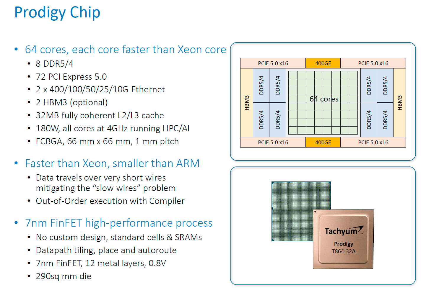
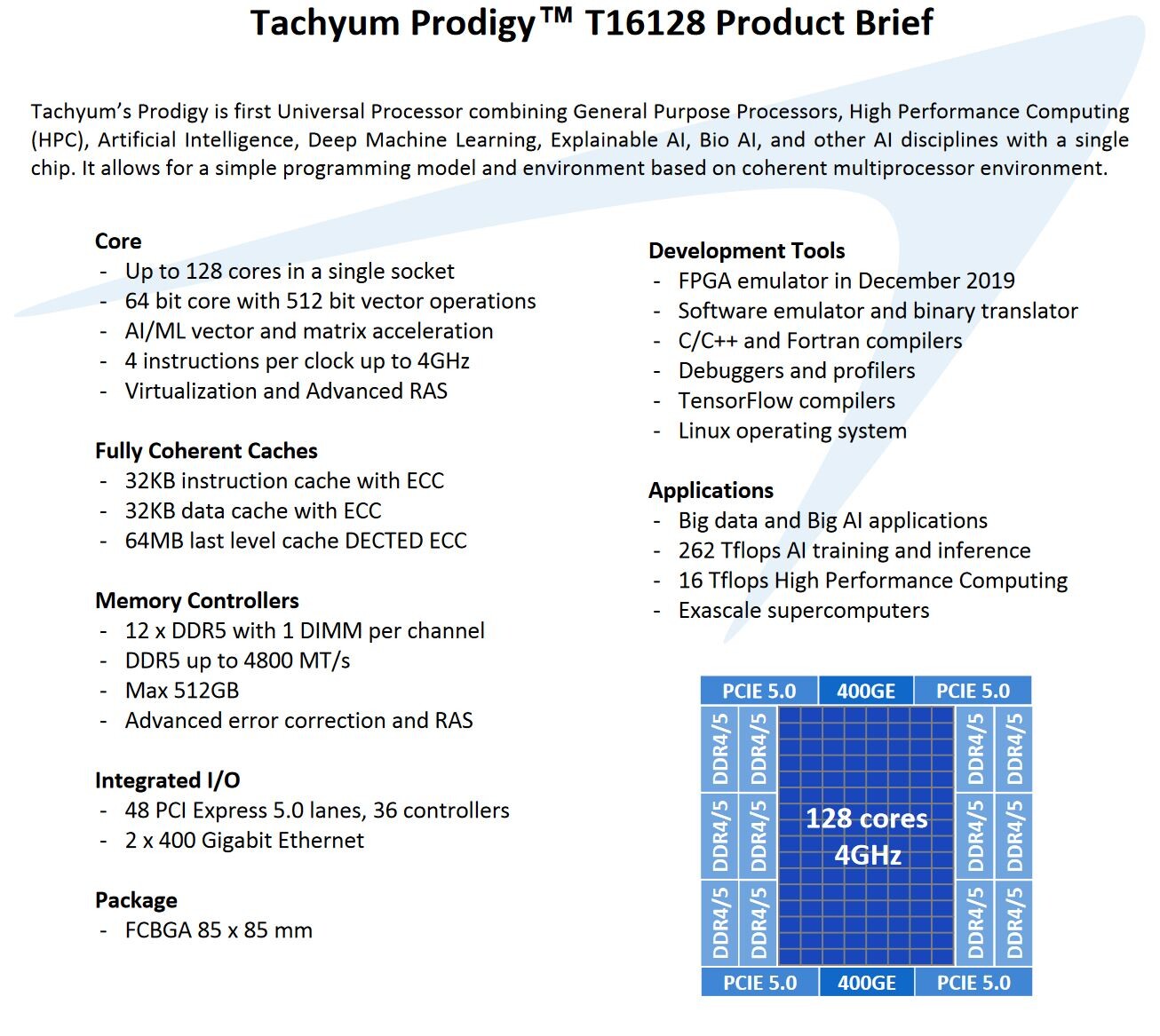
To begin with, its top trim, the Prodigy T16128, packs 128 cores on a single package, complete with 64-bit address space, 512-bit vector extensions, matrix multiplication fixed-function hardware that accelerate AI/ML, and 4 IPC at up to 4.00 GHz core clock. Tachyum began the processor's software-side support, with an FPGA emulator in December 2019 (so you can emulate the processor on an FPGA and begin developing for it), C/C++ and Fortran compilers; debuggers and profilers, tensorflow compilers, and a Linux distribution that's optimized it. The I/O capabilities of this chip are something else.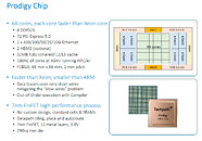
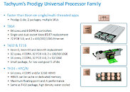
 For starters, the chip features two 400 Gbps PHYs integrated, along with a PCI-Express gen 5.0 x48 root-complex split between four SerDes. It also has a gargantuan 12-channel DDR5 memory interface (albeit limited to 1 DIMM per channel, and 512 GB cumulative memory size).
For now, Tachyum has two performance claims for the T16128. 16 TFLOPs HPC throughput (likely single-precision), and 262 TFLOPs (equivalent) AI training and inference performance, thanks to its matrix multipliers integrated into the core.
All of this crams into a 65 mm x 65 mm FCBGA package with an integrated heatspreader (slightly bigger than LGA2066 package, although smaller than an SP3 package). Underneath the IHS, the die has been fabricated on TSMC 7 nm process.
Tachyum has reportedly already taped out a smaller 64-core variant of this chip, the Prodigy T864. It features a slightly different I/O, with an 8-channel DDR4/DDR5 memory interface, an optional HBM3 interface, a wider 72-lane PCI-Express gen 5.0 root complex, and two 400 Gbps PHY interfaces. Built on the 7 nm process like its 128-core sibling, this chip's die measures 290 mm², and has a TDP rating of 180 W. ComputerBase reports that the 64-core variant will enter production within 2020.
Source:
ComputerBase.de
To begin with, its top trim, the Prodigy T16128, packs 128 cores on a single package, complete with 64-bit address space, 512-bit vector extensions, matrix multiplication fixed-function hardware that accelerate AI/ML, and 4 IPC at up to 4.00 GHz core clock. Tachyum began the processor's software-side support, with an FPGA emulator in December 2019 (so you can emulate the processor on an FPGA and begin developing for it), C/C++ and Fortran compilers; debuggers and profilers, tensorflow compilers, and a Linux distribution that's optimized it. The I/O capabilities of this chip are something else.

For now, Tachyum has two performance claims for the T16128. 16 TFLOPs HPC throughput (likely single-precision), and 262 TFLOPs (equivalent) AI training and inference performance, thanks to its matrix multipliers integrated into the core.
All of this crams into a 65 mm x 65 mm FCBGA package with an integrated heatspreader (slightly bigger than LGA2066 package, although smaller than an SP3 package). Underneath the IHS, the die has been fabricated on TSMC 7 nm process.
Tachyum has reportedly already taped out a smaller 64-core variant of this chip, the Prodigy T864. It features a slightly different I/O, with an 8-channel DDR4/DDR5 memory interface, an optional HBM3 interface, a wider 72-lane PCI-Express gen 5.0 root complex, and two 400 Gbps PHY interfaces. Built on the 7 nm process like its 128-core sibling, this chip's die measures 290 mm², and has a TDP rating of 180 W. ComputerBase reports that the 64-core variant will enter production within 2020.
51 Comments on Tachyum Prodigy is a Small 128-core Processor with Crazy I/O Options, 64-core Sibling Enroute Production
www.asml.com/en/company/about-asml/locationsMore
www.asml.com/en/company/about-asml/organizationBut the point is, it's a Dutch company.