Monday, May 11th 2020

Intel Core i9-10900K Stressed, Package Power Reads 235W, Temperatures 93°C
A stock Intel Core i9-10900K 10-core processor was subjected to FPU stress by Chinese PC enthusiast @WolStame. The power and temperature values of the processor are inside HEDT territory. With a Furmark GPU stress running on the side, under AIDA64 FPU stress, the i9-10900K measured a package power draw of up to 235.17 W, as measured using HWInfo64. The CPU package temperature shot up to 93 °C. A 240 mm AIO liquid CPU cooling solution was used in the feat. Interestingly, the processor is able to sustain clock speeds of 4.77 GHz, which is close to the advertised 4.80 GHz all-core turbo boost frequency, called for by the multi-core FPU stress.
To show that the values weren't obtained in a few seconds of test, the AIDA64 Stability Test window keeps a timestamp log and displays time elapsed into the stress. In this particular case, the all-core stress has been running for close to 48 minutes; and yet the processor is keeping up with its advertised all-core boost speed, making this an impressive feat.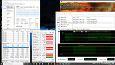
Sources:
@WolStame (Weibo), @9550pro (Twitter)
To show that the values weren't obtained in a few seconds of test, the AIDA64 Stability Test window keeps a timestamp log and displays time elapsed into the stress. In this particular case, the all-core stress has been running for close to 48 minutes; and yet the processor is keeping up with its advertised all-core boost speed, making this an impressive feat.

110 Comments on Intel Core i9-10900K Stressed, Package Power Reads 235W, Temperatures 93°C
As for the video encoding/transcoding, especially so if the video encoder is using AVX instructions like most of them do.
but 10fps extra in fortnite 1080p is worth it :laugh:
Since you brought it up though, I dont find many activities that are harder on a cpu than this or regeneration's overkill stress testing app. Stress in p95 using avx is also difficult to surpass rendering and encoding. VMs.. that is clearly situation dependent. I can spin up a few and have them do nothing. I get your point but few real world applications touch some of these stress test loads.
I've heard a story of 5.2 ghz 1.35V, all c/t passing default aida64 at 100C with a 360 aio. These things are built to take it with a TJmax of 115C.
But with my 7960x (16c/32t) 4.5 GHz 1.2V I manage to pull more, lol.
[/QUOTE]
The best traditional OC I can do is 4.175 @ 1.3.
~4.2.. not bad!
It has a much higher boiling point.
A 360mm aio liquid cooler should be sufficient. They have around 300W tdp.
I have a 120mm aio liquid cooler with 200W tdp for my i9-9900K, because of the case I am using. That is hardly enough.
I have set PL1 to 125W and PL2 to 160W.
Ryzen in full load at 70C - boiling hot
Intel CPU in full load at 100C -a bit hot.
As for the 30 MHz difference, that is not correct; as I mentioned earlier, Task manager doesn't read it correctly. Seeing as the memory in HWINFO is 1463.4 MHz, or roughly 2926.8, which is basically 2933, the reason the clock speed is lower is because of spread spectrum. (2926.8/2933) * 100 = ~99.79 MHz, which is something you will normally see in CPU Z, and that's the BCLK. that multiplied by 48x is 4789.8 MHz, which is just shy of 10 MHz. So not only I just proved Task Manager is incorrect for determining the actual clock speed (it is a small difference between actual clock speed and what task manager is showing in this case), I just showed you how to calculate a processor's clock speed. BCLK x Multiplier = Core clock speed. But seriously, something like 10-30 MHz in clock speed variance from BCLK shouldn't be what your buying decision is based on unless you are a professional overclocker.I think I have an explanation for why the 10900K is running hotter than expected. Remember how Intel is using thin die sTIM now?
Here is the problem, the IHS is thicker. Had they raised the SOCKET a little bit higher and had the prior IHS, there would be less material to go through to the cooler and it would be cooled more effectively. Delidding the CPU and using direct die cooling has been seen to greatly improve temperatures, because one less barrier is in the way, which also can mean having a bigger material barrier will not transfer heat as effectively. What Intel chose to do is compensate the thinner die with a thicker IHS, and I think the better route would have been to compensate the thinner die with a lifted up socket.
That said, I highly doubt that is the issue here. We've added 25% more cores and a TDP(lol) of 125W. These, period, are more difficult to cool. They also have an increased TJmax (115C vs 100C).
The substrate/PCB size remains the same (or is thicker?). Look at the slide. What is thinner is the die itself, not the PCB which is what warped and cracked/what you are talking about.
The thinner chip even enhances the heat conduction.