Monday, November 16th 2020

TSMC Achieves Major Breakthrough in 2 nm Manufacturing Process, Risk Production in 2023

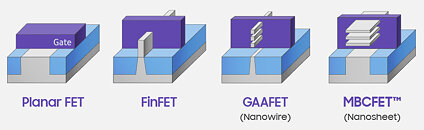
The Taiwan Economic Daily claims that TSMC has achieved a major internal breakthrough for the eventual rollout of 2 nm fabrication process technology. According to the publication, this breakthrough has turned TSMC even more optimistic towards a 2023 rollout of 2 nm risk production - which is all the more impressive considering reports that TSMC will be leaving the FinFet realm for a new multi-bridge channel field effect transistor (MBCFET) architecture - itself based on the Gate-All-Around (GAA) technology. This breakthrough comes one year after TSMC put together an internal team whose aim was to pave the way for 2 nm deployment.

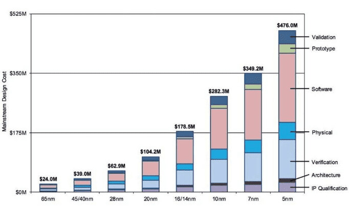
MBCFET expands on the GAAFET architecture by taking the Nanowire field-effect transistor and expanding it so that it becomes a Nanosheet. The main idea is to make the field-effect transistor three-dimensional. This new complementary metal oxide semiconductor transistor can improve circuit control and reduce leakage current. This design philosophy is not exclusive to TSMC - Samsung has plans to deploy a variant of this design on their 3 nm process technology. And as has been the norm, further reductions in chip fabrication scale come at hefty costs - while the development cost for 5 nm has already achieved $476M in cost, Samsung reports that their 3 nm GAA technology will cost in excess of $500M - and 2 nm, naturally, will come in even costlier than that.


Source: Gizchina
Add your own comment

39 Comments on TSMC Achieves Major Breakthrough in 2 nm Manufacturing Process, Risk Production in 2023

#26
Nephilim666
Optical guy here, the issue with anything past EUV is it cannot be focused anywhere near the precision of EUV. Look at Chandra and the terrible resolution it gathers in x-ray versus what Hubble can do in EUV. X-Rays ignore most matter including the exotic mirrors (some are basically diamond coated) used to focus EUV.
Posted on Reply
#27
lexluthermiester
tabascosauzI mean, true, but do we need it to be?
Yes, you're making some very big assumptions there. For one, Taiwan is not under the restrictions imposed by trade embargo and two, there is a strategic tax advantage to having a manufacturing facility stateside.
Posted on Reply
#28
BArms
Minus InfinityI wonder what my old solid state physics lecturer would say reading this. I remember being taught once we got below 10nm all hell would break loose and we'd need entirely new form of solid state devices. Line traces would be too small to stop quantum tunnelling of electrons and devices couldn't operate. 2nm seems surreal for architecture that's only several atoms in size. The physics of current transport must be highly affected as the size gets so small. I honestly didn't expect us to keep going much longer after 10nm.
It's just a marketing name, there is nothing actually 7nm about their "7nm" node and "2nm" won't be any closer to reality either.
Posted on Reply
#29
TumbleGeorge
I wish companies to use old nodes 16nm or 22nm or 28nm. It's heat density is less and more easily for cooling :D
Posted on Reply
#30
lexluthermiester
BArmsIt's just a marketing name, there is nothing actually 7nm about their "7nm" node and "2nm" won't be any closer to reality either.
No, that's not true. The "7nm" refers to the dimensional size of the smallest component within the structure of an individual computing unit. The same will be said of the "2nm" as the smallest nanosheet of the "MBCFET " process will only be 2nm thick. So the nanometer classification labels are correct within the context of their definitions. This is where a lot of the confusion comes from.

For example, with Intel's 14nm+++ etc line up, they keep getting blasted for not making more progress sooner and yet that process has product what was widely considered the fastest silicon in the world until just recently with AMD's Zen3. The refinements Intel made where solid and enough to keep them in the lead. It is only know that they need to kick things up a notch or two to match AMD's/TSMC's new hotness. Intel's new 10nm process will likely meet that challenge, but even if they stay in second they're not lagging behind by much. So even though it a 10nm process, it's still competitive with the 7nm, 5nm and so on offer elsewhere. Intel's not the performance king currently, but that will not last. They will make strides forward and then others with make their advances. This is how the games has been played for decades. It will continue..
Posted on Reply
#31
BArms
lexluthermiesterNo, that's not true. The "7nm" refers to the dimensional size of the smallest component within the structure of an individual computing unit. The same will be said of the "2nm" as the smallest nanosheet of the "MBCFET " process will only be 2nm thick. So the nanometer classification labels are correct within the context of their definitions. This is where a lot of the confusion comes from.
That hasn't been true for at least 15 years. There is nothing about a TSMC "7nm" transistor that measures 7nm.
Posted on Reply
#32
mtcn77
BArmsThat hasn't been true for at least 15 years. There is nothing about a TSMC "7nm" transistor that measures 7nm.
What about transistor fin distance? I think I know what the definition is. They do it to reach max process fidelity. You cannot lithographically get any finer than the process designation.
Posted on Reply
#33
lexluthermiester
BArmsThat hasn't been true for at least 15 years.
Rubbish.
BArmsThere is nothing about a TSMC "7nm" transistor that measures 7nm.
Also rubbish. Complete and utter nonsense.
Posted on Reply
#34
medi01
Let's remember that TSMC 7nm EUV transistor is 22 by 22nm, while 14nm+++ Intel transistor is 24 by 24nm, cough.
(as measured by some German dude, who compared L1 cache in particular)

2nm should be... around 18nm I guess.... :D
Posted on Reply
#35
lexluthermiester
medi01Let's remember that TSMC 7nm EUV transistor is 22 by 22nm, while 14nm+++ Intel transistor is 24 by 24nm, cough.
(as measured by some German dude, who compared L1 cache in particular)

2nm should be... around 18nm I guess.... :D
Actually, that sounds about right.
Posted on Reply
#36
Hossein Almet
medi01Let's remember that TSMC 7nm EUV transistor is 22 by 22nm, while 14nm+++ Intel transistor is 24 by 24nm, cough.
(as measured by some German dude, who compared L1 cache in particular)

2nm should be... around 18nm I guess.... :D
If this is true, Intel architecture is not that great, after all.
Posted on Reply
#37
mtcn77
They should measure the fin width for an accurate comparison.
Posted on Reply
#38
lexluthermiester
Hossein AlmetIf this is true, Intel architecture is not that great, after all.
Except that it was king of the performance hill until Zen3. Performance is what counts, how something is made is of a secondary concern.
Posted on Reply
#39
mtcn77
lexluthermiesterExcept that it was king of the performance hill until Zen3. Performance is what counts, how something is made is of a secondary concern.
Have you looked at this? I won't be the judge whether this guy knows his beef, but there are some yield benchmarks to the dismay of fanbots of a very vocal community.
Posted on Reply
Add your own comment
Nov 19th, 2026 19:35 CST change timezone

New Forum Posts

Popular Reviews

TPU on YouTube

Controversial News Posts