Monday, November 16th 2020

TSMC Achieves Major Breakthrough in 2 nm Manufacturing Process, Risk Production in 2023

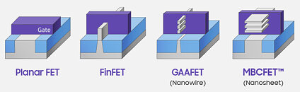
The Taiwan Economic Daily claims that TSMC has achieved a major internal breakthrough for the eventual rollout of 2 nm fabrication process technology. According to the publication, this breakthrough has turned TSMC even more optimistic towards a 2023 rollout of 2 nm risk production - which is all the more impressive considering reports that TSMC will be leaving the FinFet realm for a new multi-bridge channel field effect transistor (MBCFET) architecture - itself based on the Gate-All-Around (GAA) technology. This breakthrough comes one year after TSMC put together an internal team whose aim was to pave the way for 2 nm deployment.

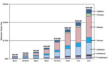
MBCFET expands on the GAAFET architecture by taking the Nanowire field-effect transistor and expanding it so that it becomes a Nanosheet. The main idea is to make the field-effect transistor three-dimensional. This new complementary metal oxide semiconductor transistor can improve circuit control and reduce leakage current. This design philosophy is not exclusive to TSMC - Samsung has plans to deploy a variant of this design on their 3 nm process technology. And as has been the norm, further reductions in chip fabrication scale come at hefty costs - while the development cost for 5 nm has already achieved $476M in cost, Samsung reports that their 3 nm GAA technology will cost in excess of $500M - and 2 nm, naturally, will come in even costlier than that.
Source: Gizchina
Add your own comment

39 Comments on TSMC Achieves Major Breakthrough in 2 nm Manufacturing Process, Risk Production in 2023

#1
Chrispy_
Man, it must suck to work for Intel and read news like this at the moment.

Competition hotting up in the race to 2nm and 3nm whilst your 10nm process is still so broken that you can't scale it up to desktops and servers, and your PHB's put all the eggs in the 7nm basket which has already been pushed back by more time that its total development cycle was supposed to last.
Posted on Reply
#2
GeorgeMan
Soo, what comes next? 0nm? And after that -1nm? As they continue to shrink the nodes, numbers are starting to become silly... We all know 7nm aren't really 7nm.
Posted on Reply
#3
Chrispy_
GeorgeManSoo, what comes next? 0nm? And after that -1nm? As they continue to shrink the nodes, numbers are starting to become silly... We all know 7nm aren't really 7nm.
I guess these half-node shrinks from TSMC and Samsung are going to need to be named differently soon as gate lengths are already pretty meaningless and soon they're going to run out of integers.
Posted on Reply
#4
HammerOn1024
GeorgeManSoo, what comes next? 0nm? And after that -1nm? As they continue to shrink the nodes, numbers are starting to become silly... We all know 7nm aren't really 7nm.
Yea... no. What's next is picometers: 1 x 10^-12. So, 999 pm is 0.999 um, etc.

So any optical guys out there know when one would have to transition from EUV light to x-rays lithography?
Posted on Reply
#5
GeorgeMan
HammerOn1024Yea... no. What's next is picometers: 1 x 10^-12. So, 999 pm is 0.999 um, etc.
I know, I was just being sarcastic about the marketing numbers we are currently being served. :)
Posted on Reply
#6
Mouth of Sauron
Well, INTEL in particular is the last "entity" (or whatever) who can complain about these naming gimmicks... Weren't they the first ones using innovative naming convention with 486DX-4, where four was indicator for CPU working 4 times faster than MB... In this concrete example, 100Mhz over 33Mhz - makes it four, right?

All similarly bad practices confuse... well, suppose everyone - something may be 2nm, but we are lead to believe that it's... 7 times better than 14nm - which I seriously doubt...
Posted on Reply
#7
bonehead123
Well, a few years ago, while visiting the Gaza pyramids,I picked up a few .000000001pm chips from some weird-looking, triangle shaped guys there, and they said they would be releasing them to this world ~2036, so we don't have too much longer to wait for some major advancements in speed, efficiency, and thermals, hahaha :)
Posted on Reply
#8
birdie
GeorgeManSoo, what comes next? 0nm? And after that -1nm? As they continue to shrink the nodes, numbers are starting to become silly... We all know 7nm aren't really 7nm.
These are marketing nanometers. They have meant crap for the past five years.

What they need to talk about and show us is density (millions of transistors per square millimeter), power consumption and frequency.
Posted on Reply
#9
Space Lynx
Astronaut
So why are they building a 5nm factory in Arizona that won't be finished until 2024? this makes no sense to me, just build a 2nm facility.... since construction hasn't even really started yet it would be easy to do...
Posted on Reply
#10
mtcn77
This is kinda big. MBCFET is the end game.
Posted on Reply
#11
repman244
lynx29So why are they building a 5nm factory in Arizona that won't be finished until 2024? this makes no sense to me, just build a 2nm facility.... since construction hasn't even really started yet it would be easy to do...
Not every chip requires to be built on newest and greatest node you know. For example: anything used for space programs cannot use any of these nodes due to the environment (radiation, temperatures etc.).
Posted on Reply
#12
Chrispy_
repman244Not every chip requires to be built on newest and greatest node you know. For example: anything used for space programs cannot use any of these nodes due to the environment (radiation, temperatures etc.).
GloFo 12nm still alive and kicking on every Zen2/Zen3 Ryzen/TR/EPYC processor made today.
Posted on Reply
#13
BArms
Mouth of SauronWell, INTEL in particular is the last "entity" (or whatever) who can complain about these naming gimmicks... Weren't they the first ones using innovative naming convention with 486DX-4, where four was indicator for CPU working 4 times faster than MB... In this concrete example, 100Mhz over 33Mhz - makes it four, right?

All similarly bad practices confuse... well, suppose everyone - something may be 2nm, but we are lead to believe that it's... 7 times better than 14nm - which I seriously doubt...
That's actually not a good example because I know the 486 also had a 25mhz bus option. There was even an original Pentium that ran at 50mhz (2x25).
Posted on Reply
#14
Space Lynx
Astronaut
Chrispy_GloFo 12nm still alive and kicking on every Zen2/Zen3 Ryzen/TR/EPYC processor made today.
ya but context is important with a comment like this, which you fail to provide. lulz.
Posted on Reply
#15
roberto888
lynx29So why are they building a 5nm factory in Arizona that won't be finished until 2024? this makes no sense to me, just build a 2nm facility.... since construction hasn't even really started yet it would be easy to do...
Not every chip requires to be built on newest and greatest node you know. For example: anything used for space programs cannot use any of these nodes due to the environment (radiation, temperatures etc.).
Also it needs to go through a lot of testing and validation I guess, before they can roll it out.
Posted on Reply
#16
lexluthermiester
Chrispy_Man, it must suck to work for Intel and read news like this at the moment.

Competition hotting up in the race to 2nm and 3nm whilst your 10nm process is still so broken that you can't scale it up to desktops and servers, and your PHB's put all the eggs in the 7nm basket which has already been pushed back by more time that its total development cycle was supposed to last.
You do know there's more to the equation than just raw nanometer scaling statements, right?
Posted on Reply
#17
Chrispy_
lexluthermiesterYou do know there's more to the equation than just raw nanometer scaling statements, right?
I've already said as much in this very thread:
Chrispy_gate lengths are already pretty meaningless
It's just a node name and one of the reason Intel's 10nm is doing so badly is because it's trying more new/risky technologies than TSMC's 7nm and it's actually pretty close in transistor density as well.

If Intel had been less ambitious with 10nm and just worked on a simpler jump, (ie, still 10nm but not trying multiple high-risk industry-firsts like Cobalt, COAG, and 36nm pitch without EUV) they likely wouldn't be in the mess they're in right now.
Posted on Reply
#18
tabascosauz
lynx29So why are they building a 5nm factory in Arizona that won't be finished until 2024? this makes no sense to me, just build a 2nm facility.... since construction hasn't even really started yet it would be easy to do...
The US fab is not for you and me. The US fab is for government and military contracts. TSMC wants to get on the Trusted Foundry list and take government business away from Globalfoundries' two fabs, with its cutting edge (in the military context) processes.
Posted on Reply
#19
lexluthermiester
tabascosauzThe US fab is not for you and me. The US fab is for government and military contracts. TSMC wants to get on the Trusted Foundry list and take government business away from Globalfoundries' two fabs, with its cutting edge (in the military context) processes.
That has not, as of yet, been confirmed publicly.
Posted on Reply
#20
laszlo
milking the nm cow til possible this is all; when they reach the physical limit game over; in 5 years if no other solution will become viable we'll be stuck at multi chip level to compensate ....
Posted on Reply
#21
tabascosauz
lexluthermiesterThat has not, as of yet, been confirmed publicly.
I mean, true, but do we need it to be? It's not an inexpensive fab to build, but in size and supply it's nowhere near the size it would need to be at to rival or meaningfully supplement TSMC's existing "consumer-facing" fabs, and TSMC's own expected roadmaps would leave N5 in the dust in a consumer electronics context. On the other hand, even considering the increasing popularity of COTS and modern electronics in new military projects, applying the N5 process would be a big step up for military contracts, especially given the US' current objectives with respect to China. They've got a lot of work to do on the technology front, and the new US fab seems all but geared towards that.
Posted on Reply
#22
TumbleGeorge
laszlomilking the nm cow til possible this is all; when they reach the physical limit game over; in 5 years if no other solution will become viable we'll be stuck at multi chip level to compensate ....
Gates lenght is XXnm far away from it's physical limits. Marketing nanometers is only how wight(fat) is transistor itself. That in not related to physical limitations of node.

credit: extremetech+wikichip
Posted on Reply
#23
hardcore_gamer
birdieThese are marketing nanometers. They have meant crap for the past five years.

What they need to talk about and show us is density (millions of transistors per square millimeter), power consumption and frequency.
No 2nm info yet, but here are some estimates from WikiChip for TSMCs 5 and 3nm:


Density will continue to scale well and the power consumption will decrease a bit, however with Dennard scaling hitting a wall, don't expect any significant increases in clock frequencies. CPU architectures will have to go wider and deeper to increase single core performance. GPUs can have significant performance increases by having more execution units at almost the same or even lower clocks.
HammerOn1024So any optical guys out there know when one would have to transition from EUV light to x-rays lithography?
Not an optical guy, but as a device architect, I don't think it'll happen for silicon. Multipatterning EUV is enough to hit the limitations of silicon. We'll see short channel effects making silicon unsuitable for any further scaling before the need for x-ray lithography arises. 3D stacking can extend the life of silicon for a little bit longer, before moving to alternate materials.
Posted on Reply
#24
Hossein Almet
That's why I order the 5950X now instead of waiting for the zen 4, so that in 6 or 7 years time I'll move to the 2nm note.
Posted on Reply
#25
Minus Infinity
I wonder what my old solid state physics lecturer would say reading this. I remember being taught once we got below 10nm all hell would break loose and we'd need entirely new form of solid state devices. Line traces would be too small to stop quantum tunnelling of electrons and devices couldn't operate. 2nm seems surreal for architecture that's only several atoms in size. The physics of current transport must be highly affected as the size gets so small. I honestly didn't expect us to keep going much longer after 10nm.
Posted on Reply
Add your own comment
Apr 25th, 2024 10:08 EDT change timezone

New Forum Posts

Popular Reviews

Controversial News Posts