Tuesday, August 30th 2022

AMD "Zen 4" Dies, Transistor-Counts, Cache Sizes and Latencies Detailed
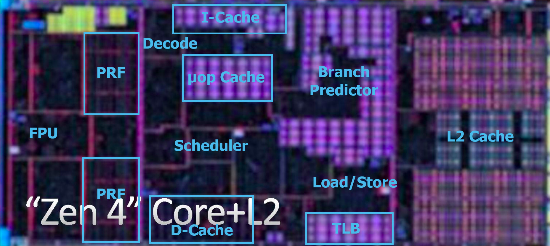
As we await technical documents from AMD detailing its new "Zen 4" microarchitecture, particularly the all-important CPU core Front-End and Branch Prediction units that have contributed two-thirds of the 13% IPC gain over the previous-generation "Zen 3" core, the tech enthusiast community is already decoding images from the Ryzen 7000 series launch presentation. "Skyjuice" presented the first annotation of the "Zen 4" core, revealing its large branch-prediction unit, enlarged micro-op cache, TLB, load/store unit, and dual-pumped 256-bit FPU that enables AVX-512 support. A quarter of the core's die-area is also taken up by the 1 MB dedicated L2 cache.
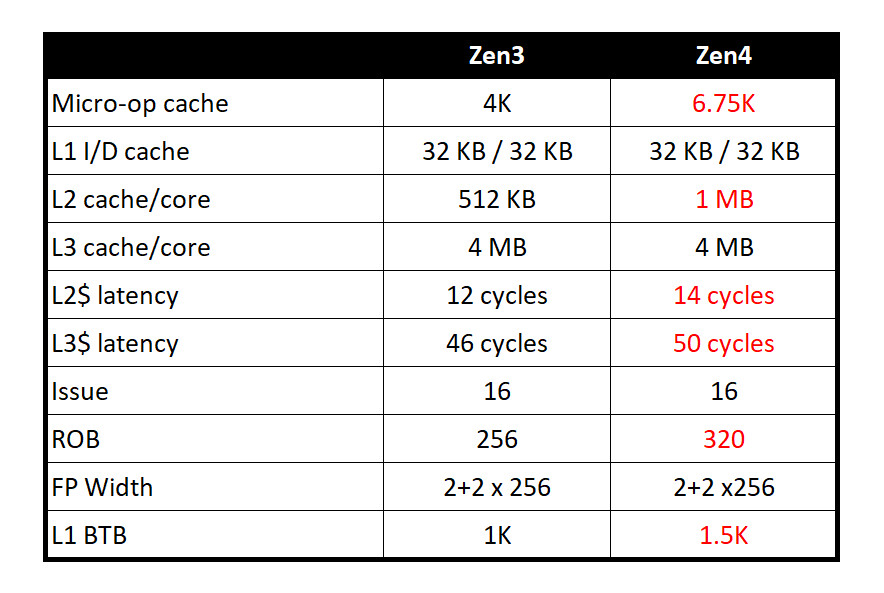
Chiakokhua (aka Retired Engineer) posted a table detailing the various caches and their latencies, comparing it with those of the "Zen 3" core. As AMD's Mark Papermaster revealed in the Ryzen 7000 launch event, the company has enlarged the micro-op cache of the core from 4 K entries to 6.75 K entries. The L1I and L1D caches remain 32 KB in size, each; while the L2 cache has doubled in size. The enlargement of the L2 cache has slightly increased latency, from 12 cycles to 14. Latency of the shared L3 cache is also up, from 46 cycles to 50 cycles. The reorder buffer (ROB) in the dispatch stage has been enlarged from 256 entries to 320 entries. The L1 branch target buffer (BTB) has increased in size from 1 KB to 1.5 KB.
 The Zen 4 CCD is slightly smaller than the Zen 3 CCD despite the higher transistor-counts, thanks to the switch to 5 nm (TSMC N5 process). The CCD measures 70 mm², in comparison to the 83 mm² "Zen 3" CCD. The transistor-count of the "Zen 4" CCD is 6.57 billion, a whopping 58 percent increase from that of the "Zen 3" CCD and its 4.15 billion transistor-count.
The cIOD (client I/O die) sees a big chunk of innovation. It's built on the 6 nm (TSMC N6) node, which is a big leap from the GlobalFoundries 12 nm node that the cIOD of Ryzen 5000 series processors were made on. It also incorporates certain power-management features from the Ryzen 6000 "Rembrandt" processors. This cIOD packs an iGPU based on the RDNA2 graphics architecture, besides the DDR5 memory controllers, and a PCI-Express Gen 5 root complex. The new 6 nm cIOD measures 124.7 mm², compared to the slightly larger 124.9 mm² cIOD of the Ryzen 5000 series.
The "Raphael" multi-chip module has one CCD for the 6-core and 8-core SKUs, and two CCDs for the 12-core and 16-core SKUs. "Raphael" is built in the Socket AM5 package. AMD is rumored to be readying a thin BGA package of "Raphael" for high-performance notebook platforms, which it's codenamed "Dragon Range." These processors will come in various 45 W, 55 W, and 65 W TDP points, powering high-end gaming notebooks.
Sources:
Chiakokhua (Twitter), Skyjuice (Twitter), Skyjuice (Angstronomics)
Chiakokhua (aka Retired Engineer) posted a table detailing the various caches and their latencies, comparing it with those of the "Zen 3" core. As AMD's Mark Papermaster revealed in the Ryzen 7000 launch event, the company has enlarged the micro-op cache of the core from 4 K entries to 6.75 K entries. The L1I and L1D caches remain 32 KB in size, each; while the L2 cache has doubled in size. The enlargement of the L2 cache has slightly increased latency, from 12 cycles to 14. Latency of the shared L3 cache is also up, from 46 cycles to 50 cycles. The reorder buffer (ROB) in the dispatch stage has been enlarged from 256 entries to 320 entries. The L1 branch target buffer (BTB) has increased in size from 1 KB to 1.5 KB.
The cIOD (client I/O die) sees a big chunk of innovation. It's built on the 6 nm (TSMC N6) node, which is a big leap from the GlobalFoundries 12 nm node that the cIOD of Ryzen 5000 series processors were made on. It also incorporates certain power-management features from the Ryzen 6000 "Rembrandt" processors. This cIOD packs an iGPU based on the RDNA2 graphics architecture, besides the DDR5 memory controllers, and a PCI-Express Gen 5 root complex. The new 6 nm cIOD measures 124.7 mm², compared to the slightly larger 124.9 mm² cIOD of the Ryzen 5000 series.
The "Raphael" multi-chip module has one CCD for the 6-core and 8-core SKUs, and two CCDs for the 12-core and 16-core SKUs. "Raphael" is built in the Socket AM5 package. AMD is rumored to be readying a thin BGA package of "Raphael" for high-performance notebook platforms, which it's codenamed "Dragon Range." These processors will come in various 45 W, 55 W, and 65 W TDP points, powering high-end gaming notebooks.
41 Comments on AMD "Zen 4" Dies, Transistor-Counts, Cache Sizes and Latencies Detailed
[INDENT][/INDENT]
[INDENT]Graphics Capabilities[/INDENT]
[INDENT]Graphics Model: AMD Radeon™ Graphics[/INDENT]
[INDENT]Graphics Core Count: 2[/INDENT]
[INDENT]Graphics Frequency: 2200 MHz[/INDENT]
[INDENT]GPU Base: 400 MHz[/INDENT]
Based in the info above, it should have around 560 GFLOPS of compute.
Vega 11, in the 5700G, has 2.048 TFLOPS. Expect around 1/4 the performance.
Obviously, the move to DDR5 could offset the reduction slightly, but it is best to wait for the APU's.
EDIT: logic fail
If you take 58% divide by 8 gives 7,25%So 7% transistor increase per core for 13% IPC per core increase?
That's 186% gain per transistor increase.
Didn't they say ~50% multi-core perf increase over last gen at same power? Sounds pretty reasonable if you include the clockspeed improvements, double AVX execution, increased cache.
But you are somewhat correct that we shouldn't look at IPC vs transistors, because transistors also enable higher clocks, and possibly better multithreaded perf, so we should look at that ~50% overall performance boost.
That's still just half the truth because it's not on same production node, so part of frequency uptake is also due to 5nm.
So 58% transistors probably equate to ~30% performance.
But it certainly doesn't work the way you suggest, 58/8=7.25 is correct, but doing so with % is incorrect.
The process node helps but iirc the design needs to be changed to actually take advantage of the new node VF curve, otherwise you only gain density improvements
It is slow in CinebenchR23 because of this desgin choice. Although I remeber a lontime ago Intel's AVX has the ablity to push AVX's up from the old to highest newest version in the cpu to improve speed, athough it was also in that same pdf I read that it would take SSE4.1 to AVX. Mysterly after I asked a question abou that to a fameous intel Engineer the PDF disappered off from view.
www.mersenneforum.org/showthread.php?p=614191
a Native AVX512 would use more power be hotter & clock lower