Sunday, August 6th 2023

AMD Retreating from Enthusiast Graphics Segment with RDNA4?

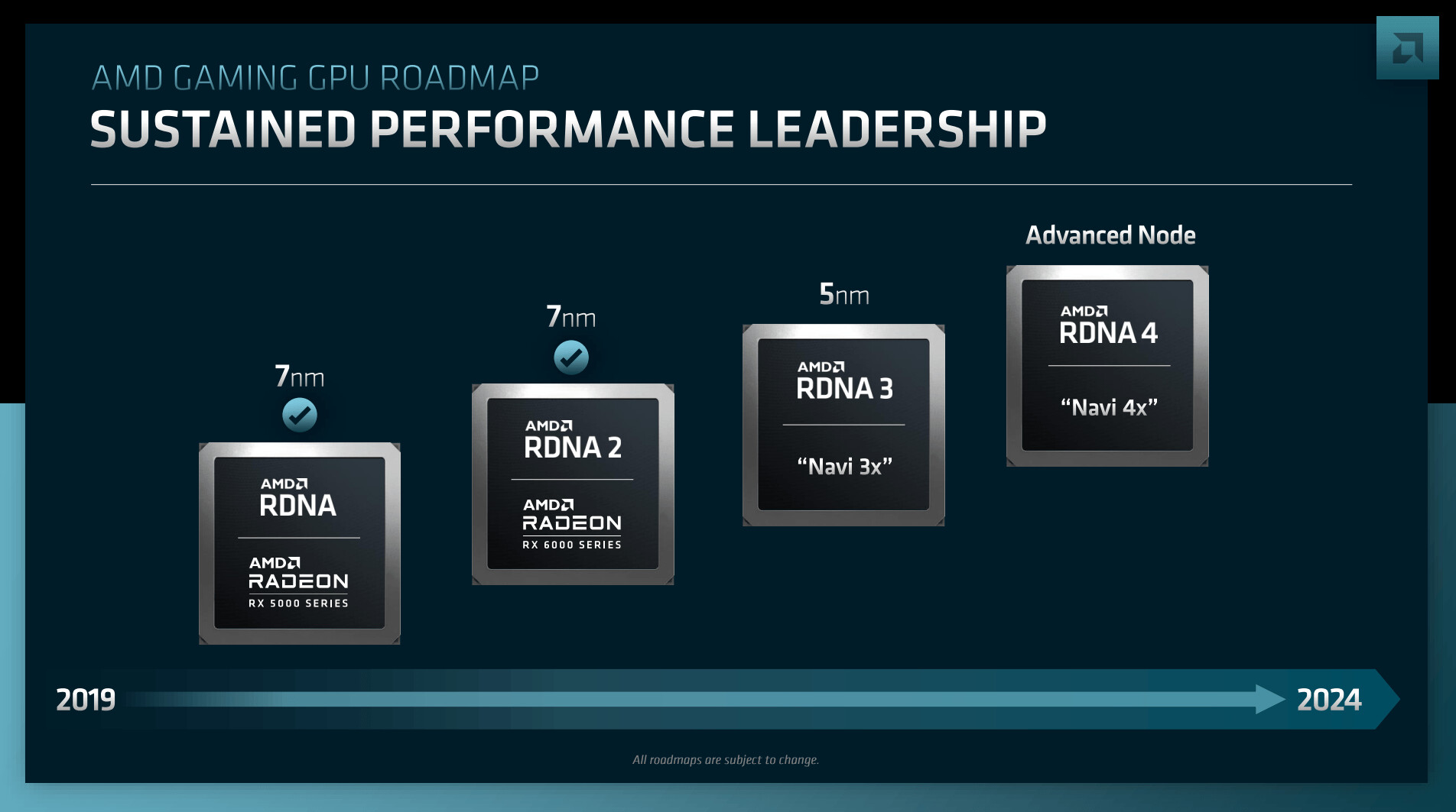
AMD is rumored to be withdrawing from the enthusiast graphics segment with its next RDNA4 graphics architecture. This means there won't be a successor to its "Navi 31" silicon that competes at the high-end with NVIDIA; but rather one that competes in the performance segment and below. It's possible AMD isn't able to justify the cost of developing high-end GPUs to push enough volumes over the product lifecycle. The company's "Navi 21" GPU benefited from the crypto-currency mining swell, but just like with NVIDIA, the company isn't able to push enough GPUs at the high-end.

With RDNA4, the company will focus on specific segments of the market that sell the most, which would be the x700-series and below. This generation will be essentially similar to the RX 5000 series powered by RDNA1, which did enough to stir things up in NVIDIA's lineup, and trigger the introduction of the RTX 20 SUPER series. The next generation could see RDNA4 square off against NVIDIA's next-generation, and hopefully, Intel's Arc "Battlemage" family.
Source: VideoCardz
Add your own comment

363 Comments on AMD Retreating from Enthusiast Graphics Segment with RDNA4?

#326
Tek-Check
ViperXZThat being said, btt, I'm still not 100% sold that AMD will skip the enthusiast (high margin) market for RDNA 4 - rumors are just rumors, and rumors can also change opinions (of AMD).
One of
ARFBut nvidia's market cap is 1 trillion, while AMD is much smaller - only ~173 billion.
I think this is a severe mismanagement on AMD's side. They should stop the development of CPUs, and instead focus 100% on the GPUs - there is much more money in it
Mismanagement? Hahaha. If that was the case, Lisa Su and other senior leaders would have been easily sacked long time ago. I hope you are not saying that it's difficult to change bosses of tech companies in America, are you?

Market cap can be very volatile and unstable measure of company value. It often goes up and down in waves and cycles, for various reasons. It's more a measure of investor's momentary estimate of a business. If you take a look below, you will see just how volatile market cap of Nvidia has been. AMD's market cap has been less volatile, which suggests more steady valuation, with less of investor hysteria. Similarly for TSMC.
companiesmarketcap.com/nvidia/marketcap/
companiesmarketcap.com/amd/marketcap/
companiesmarketcap.com/tsmc/marketcap/

There is currently more money in server GPUs for AI craze, but we don't know how long this is going to last. Nvidia leads here, which is fine, but that does not mean it would be the same in a few years. Plus, AMD is heavily investing in server GPUs - Instinct MI300 series and they are testing already MI400 in labs. So, nothing to worry about. They are fine and healthy. Steady strategy, no hysteria.
ARFRTG needs more autonomy inside AMD. AMD should be two companies under one roof - Ryzen Technology Group and Radeon Technology Group. In this case, both parts will have equal opportunities and equal starts. Today, RTG is left on an autopilot, and of course, the only thing which lead from it is downward spiralling...
This does not make sense, as both CPU and GPU divisions actually closely work together. The result - extremely promising MI300 Instinct and other APUs. It's only going to get better as they slowly muscle their way into AI market. Steady.
ARFIt is a critical mistake to rely only on one supplier - in this case only TSMC. There must always be diversification.
Tell that to Apple and Nvidia. They don't have problems, do they? There are always Intel and Samsung around for chips that do not need to be on cutting edge node.
Plus, you might have been around to read news that several new megafabs are being built in the US and Europe by TSMC, Intel and Samsung.
ARFI thought GLOBALFOUNDRIES and AMD share the same owners.
No. GloFo explicitly decided to focus on DUV litography as they do not have interest and capacity to pursue EUV era of chip making.
Only five companies have enough resources and expertise for EUV era - Intel, Samsung, TSMC, Micron and SK Hynix.
ViperXZ35B (it's actually 52B) is a lot, but they get a whole company for that, not just "a node" with some exclusive availability that later then gets shared with other companies, that are basically competitors (unlike with Apple).
Exactly. Xilinx was a strategic move, as AMD acquired a lot of IP and device designs for server and AI era, such as FPGAs, DPUs, media encoders, embedded solutions, etc. This division has skyrocketed in revenues in last finantial report for Q2 2023. Great asset.
Posted on Reply
#327
ARF
Tek-CheckThis does not make sense, as both CPU and GPU divisions actually closely work together. The result - extremely promising MI300 Instinct and other APUs.
I can see neither the "promising" MI300 nor the APUs. Who is the actual target of these things? I am not and billions of gamers are not, too.
Posted on Reply
#328
Kapone33
For me the only reason this thread was even created are how popular AMD APUs are right now. They even put a 16 core X3D chip on laptop.
Posted on Reply
#329
rv8000
ARFI can see neither the "promising" MI300 nor the APUs. Who is the actual target of these things? I am not and billions of gamers are not, too.
Meanwhile hundreds of thousands of “gamers” are buying devices such as the steam deck, ally, ayaneo etc… and their is continued/active development.

Modern consoles are/use APUs as well. And i wouldn’t be surprised that there are plenty of deployed use cases outside of gaming for APUs that many of us aren’t aware of.

The number of people in this thread who know how to run multi billion tech companies is really amazing. What a great tech site.
Posted on Reply
#330
ViperXZ
rv8000The number of people in this thread who know how to run multi billion tech companies is really amazing. What a great tech site.
It's always possible that some of the people who talk here are actually working at the discussed companies... just some fft. ;) Don't be too sure
Posted on Reply
#331
Tek-Check
ARFI can see neither the "promising" MI300 nor the APUs. Who is the actual target of these things? I am not and billions of gamers are not, too.
You cannot see MI300 Instinct? You want to find out the actual target of these things? Wait no more.

In that case, you might want to get informed more about the company's graphics divisions and how they work together.
Graphics division has several client and server oriented teams that work on multiple architectures. They design IP for consoles, client APUs, discrete GPUs and server GPUs/APUs. Each team has their own responsibility, but they often collaborate on shared aspects of graphics, such as chiplets and compute elements for CDNA and RDNA architectures.

You might also want to learn more about server and AI products, what ships, what is sampled to customers and what would launch this year. Did you see already famous presentation for AI and data center? It's below. A lot of informative content that answer some of your questions.

AMD Data Center & AI Technology Premiere

ARF:kookoo:
AMD went in full retard mode. The gaming market will feel the pain in the coming years.
Why retard? Navi 41 looks like a very ambitious and complex project that needs more time to develop. Which makes me think that it's not surprising it might be ready for RDNA5 as Navi 51 or similar.

Wider context.
In 2025, cutting-edge high-NA EUV machines from ASML will start to ship to Intel, TSMC and Samsung. Those machines will produce chips of maximum size around ~400 mm2 and be suitable for 2nm and more advanced nodes. Due to chip size restrictions, all high compute designs on top tier client and server products will need to be designed as chiplets to be able to benefit from those future machines.

Intel, AMD and Nvidia are already designing server chiplets for 2025-2026 etching process on those machines. Those are post-RDNA4, post-Hopper and post-Ponte Vecchio designs. So, the companies need to experiment already now with those designs. Navi 41 might be just early bird in this direction, one of many designs that is tested and developed.
Posted on Reply
#332
ViperXZ
Tek-CheckIn 2025, cutting-edge high-NA EUV machines from ASML will start to ship to Intel, TSMC and Samsung. Those machines will produce chips of maximum size around ~400 mm2 and be suitable for 2nm and more advanced nodes. Due to chip size restrictions, all high compute designs on top tier client and server products will need to be designed as chiplets to be able to benefit from those future machines.
This will 100% not be the final size it can reach. Only the initial early 2nm node, maybe, but never never in the long run. In the long run it will reach much bigger sizes I will bet.
Posted on Reply
#333
AusWolf
I find it interesting how hooked up on market share some of you are. Like owning less than 50% of the graphics card market was an utter failure, not counting the size of the company, number of employees, average wage of said employees, development costs, profit margins, etc. Has it occurred to anyone that AMD might not be doing so bad in these fonts? I mean, if we suppose that I own a company of 10 people, and we all make enough money selling only 1000 items of something a year, then who's to say that we're doing worse than Nvidia?
Posted on Reply
#334
Tek-Check
ViperXZThis will 100% not be the final size it can reach. Only the initial early 2nm node, maybe, but never never in the long run. In the long run it will reach much bigger sizes I will bet.
Here is some analysis fo new ASML scanners showing restricted die size due to smaller mask. Reticle size is suggested to half on new 0.55 high-NA EUV etching scanner. It seems to be a design choice by ASML for high-volume etching process.

It makes sense, because we are seeing that all HPC chip design companies are moving their complex chips into chiplet domain because their foundaries notified them of the nature of future EUV machines. Of course, monolithic dies will remain available on current machines with lower volume throughput, but it remains to be seen which nodes will be assigned to which machines in future.


AusWolfI find it interesting how hooked up on market share some of you are. Like owning less than 50% of the graphics card market was an utter failure, not counting the size of the company, number of employees, average wage of said employees, development costs, profit margins, etc. Has it occurred to anyone that AMD might not be doing so bad in these fonts? I mean, if we suppose that I own a company of 10 people, and we all make enough money selling only 1000 items of something a year, then who's to say that we're doing worse than Nvidia?
That's exactly what I tried to explain extensively in the post #315
Posted on Reply
#335
ViperXZ
Tek-CheckHere is some analysis fo new ASML scanners showing restricted die size due to smaller mask. Reticle size is suggested to half on new 0.55 high-NA EUV etching scanner. It seems to be a design choice by ASML for high-volume etching process.
Yes but unless ASML says this is it, I won't accept that 400mm² (not exactly big) is the final size. Right now maximum size is 835mm², just for a refresher.

That being said, I never disagreed that chiplet won't be beneficial in the future, or even needed.
Posted on Reply
#336
Tek-Check
ViperXZYes but unless ASML says this is it, I won't accept that 400mm² (not exactly big) is the final size. Right now maximum size is 835mm², just for a refresher.
Design phase is completed and new machines are being built already. Intel will get the first high-NA EUV 0.55 delivery in 2025. Machine spec and ~400mm² reticle have been presented several times on official slides, like the one I posted.

The reason why each chip has ~400mm² surface is because high-NA 0.55 EUV scanner prints on half of the field in comparison to current high-NA 0.33 scanners that can print 835mm² chips. The new process increases the throughput per hour to ~185 wph (from ~160 wph), which brings ~220,000 more wafers each year. This is essential to keep prices of chips down as current machines are slower. Improved versions in 2026-2027 should print more than 220 wafers per hour.

Text by an engineer from ASML explaining the optics of high-NA EUV 0.55 and why it is economically viable and necessary.
spie.org/news/6259-improving-the-resolution-of-extreme-uv-lithography-scanners?SSO=1

Here, all explained by optical science as to why the chip area must be 16.5mm x 26mm, which gives chips up to ~400mm²

Currently, 4080 GPU is on ~380mm² chip, so it's not difficult to imagine high-tier consumer GPU on 2nm node and 400mm² die in 2026.
Posted on Reply
#337
ViperXZ
Tek-CheckDesign phase is completed and new machines are being built already. Intel will get the first high-NA EUV 0.55 delivery in 2025. Machine spec and ~400mm² reticle have been presented several times on official slides, like the one I posted.

The reason why each chip has ~400mm² surface is because high-NA 0.55 EUV scanner prints on half of the field in comparison to current high-NA 0.33 scanners that can print 835mm² chips. The new process increases the throughput per hour to ~185 wph (from ~160 wph), which brings ~220,000 more wafers each year. This is essential to keep prices of chips down as current machines are slower. Improved versions in 2026-2027 should print more than 220 wafers per hour.

Text by an engineer from ASML explaining the optics of high-NA EUV 0.55 and why it is economically viable and necessary.
spie.org/news/6259-improving-the-resolution-of-extreme-uv-lithography-scanners?SSO=1

Here, all explained by optical science as to why the chip area must be 16.5mm x 26mm, which gives chips up to ~400mm²

Currently, 4080 GPU is on ~380mm² chip, so it's not difficult to imagine high-tier consumer GPU on 2nm node and 400mm² die in 2026.
Well alright, I'm not 100% on this*, but it's a acceptable answer for now.

(*because things can change or improve)
Posted on Reply
#338
Tek-Check
ViperXZWell alright, I'm not 100% on this*, but it's a acceptable answer for now.

(*because things can change or improve)
Those parametres are established and decided upon several years ahead due to complexity and massive expense to develop machines. Once settled, they ask fabs companies to contribute financially to manufacturing process. Currently, there are a dozen orders for 0.55 High-NA EUV scanners, each costing up to $400 million.

What they can improve is throughput per hour, but not the chip size, which I also mentioned and which is on a roadmap already, so ASML must already have an experimental scanner for 220 wafers per hour
Posted on Reply
#339
ARF
Tek-CheckWhy retard? Navi 41 looks like a very ambitious and complex project that needs more time to develop.
CrossFire actually worked, but surprisingly they abandoned it.
Better return to it with "chiplets" of whatever size they want, make multi-GPU cards like the Radeon HD 7990, and call it a day.

It is a beautiful concept that was made possible and actually worked!

Posted on Reply
#340
Kapone33
ARFCrossFire actually worked, but surprisingly they abandoned it.
Better return to it with "chiplets" of whatever size they want, make multi-GPU cards like the Radeon HD 7990, and call it a day.

It is a beautiful concept that was made possible and actually worked!

Polaris were the best implementation of Crossfire and Vega was the highest performing.
Posted on Reply
#341
Dan.G
Ah, come on, now. There's no need for a high-end graphics card to watch porn...
Posted on Reply
#342
rv8000
ViperXZIt's always possible that some of the people who talk here are actually working at the discussed companies... just some fft. ;) Don't be too sure
Let me know when Gelsinger, Lisa, Cook, and Jensen decide to hop in for some casual chat then. Or anyone who actually leads a department, as they’re clearly going to discuss the inner works of their company and business strategy on a public forum.
Posted on Reply
#343
AusWolf
ARFCrossFire actually worked, but surprisingly they abandoned it.
Better return to it with "chiplets" of whatever size they want, make multi-GPU cards like the Radeon HD 7990, and call it a day.

It is a beautiful concept that was made possible and actually worked!

It worked, but large single GPUs work way better, and they don't need PCI-e splitter chips, and double the VRAM and power circuitry. x90 cards are the new CF/SLi.
Posted on Reply
#344
Eskimonster
Either they should go full Ape(u) line or continuing to try gain high end GPU market shares, half arsing it will only diminish and lessen their competitiveness. In the consumer market.
Posted on Reply
#345
ViperXZ
AusWolfx90 cards are the new CF/SLi.
They are only really the successor to the 580 780 (Ti) 980 Ti 1080 Ti 2080 Ti 3090 (Ti), so nothing special. Basically Nvidia renamed x80 Ti to xx90 and ditched Titan. Else it would still be 4080 Ti + TITAN RTXXX or whatever they would call it.
Posted on Reply
#346
RJARRRPCGP
GicaMaybe not. You don't give an example of an "OC" versus non-oc specimen. The performance/consumption ratio is clearly in nVidia's favor on all levels.
In gaming, the difference is 34W. Maximum, is 41W.
Quite embarrassing because the RX 7600 has the consumption of a 4060 Ti, and performs only in rasterization at the level of a non-ti 4060.

Wasn't GTX 1660 Ti a special case, too, where the wattage is lower than the GTX 1660 Super? Looked like there were readings indicating that.
Posted on Reply
#347
Ruru
S.T.A.R.S.
AusWolfIt worked, but large single GPUs work way better, and they don't need PCI-e splitter chips, and double the VRAM and power circuitry. x90 cards are the new CF/SLi.
Agree. I had a R9 290 CF several years ago, then I switched to a GTX 980 Ti and when it had less raw horsepower, it just worked much better. No microstuttering, no worrying for games with bad/nonexistent multi-GPU support and lower power consumption.
RJARRRPCGPWasn't GTX 1660 Ti a special case, too, where the wattage is lower than the GTX 1660 Super? Looked like there were readings indicating that.
I guess Ti had just a better binned chip with lower voltage. That would be the most reasonable reason.
Posted on Reply
#348
ViperXZ
KissamiesNo microstuttering
The microstuttering was solved when they switched to frame pacing with AMD drivers for Crossfire, so if you still had stuttering you either had frame pacing off, somehow, or the game wasn't properly supported.
Posted on Reply
#349
Ruru
S.T.A.R.S.
ViperXZThe microstuttering was solved when they switched to frame pacing with AMD drivers for Crossfire, so if you still had stuttering you either had frame pacing off, somehow, or the game wasn't properly supported.
Could be. I just remember how the difference in playability was like between day and night when I went from R9 290 CF to 980 Ti in BF1 even though the FPS was lower.
Posted on Reply
#350
ViperXZ
KissamiesCould be. I just remember how the difference in playability was like between day and night when I went from R9 290 CF to 980 Ti in BF1 even though the FPS was lower.
Yea that's typical multi-GPU stuttering for you (game not supported/no frame pacing produces this issue), fps is high but it's not producing the quality you'd expect, ie fluidity that usually gets hand in hand with high fps.
Posted on Reply
Add your own comment
Jul 8th, 2025 23:22 CDT change timezone

New Forum Posts

Popular Reviews

TPU on YouTube

Controversial News Posts