Thursday, October 5th 2023

Samsung and TSMC Reportedly Struggling with 3 nm Yields

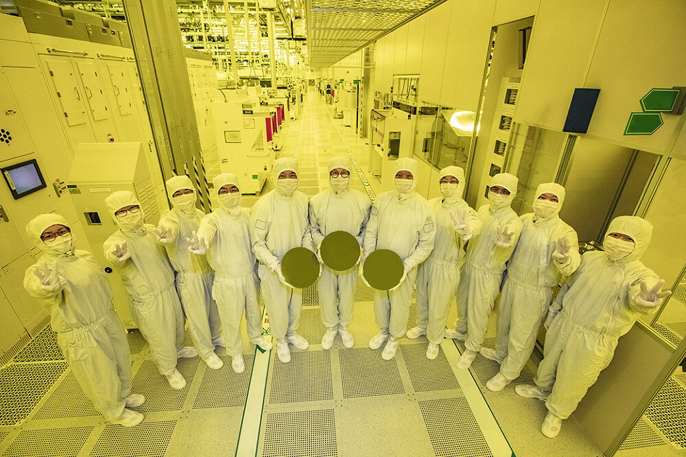
According to Korean business news publication ChosunBiz, both Samsung and TSMC are struggling with their 3 nm node yields. The two companies have different approaches to their 3 nm nodes, with Samsung using GAA FET (Gate All Around), whereas TSMC is continuing with its FinFET technology. That said, TSMC has at least five known 3 nm nodes, of which two should be in production by now, assuming N3E has proved to be reliable enough to kick off. Samsung on the other hand has three known 3 nm nodes, with only one in production so far, called 3GAE.

ChosunBiz reports that neither company is getting the kind of yields that you'd expect from a node that should have been in volume production for around a year by now, with Samsung apparently being somewhat better than TSMC. At 60 and 50 percent respectively, neither Samsung nor TSMC are anywhere near decent yields. Anything below 70 percent is considered very poor and even the 60 percent claim in Samsungs case, is apparently limited to some kind of Chinese mining ASIC and doesn't include the SRAM you find in most modern processors. ChosunBiz also mentions a source familiar with Samsung's foundry business who mentions a yield closer to 50 percent for the company. The same source also mentions that Samsung needs to reach at least 70 percent yield to be able to attract major customers to its 3 nm node.
Sources: ChosunBiz, via @Tech_Reve (on X)
Add your own comment

81 Comments on Samsung and TSMC Reportedly Struggling with 3 nm Yields

#76
bug
WirkoHm, I don't see what that could mean. The transistor is the only type of component that can be manufactured on a chip, and all are the same size (Iit can be a bit different with finfets because the process may allow a combination of two sizes, for example, half are 3-fin and the other half are 2-fin.) But you sometimes need other components in a circuit, and some transistors have to serve as capacitors or (maybe) resistors. Some transistors have to be bigger for high performance, in practice those are two or more transistors connected in parallel. The layout certainly isn't 100% optimised, so there's some unused space (but I gues designers can always put capacitors there).

Here's an article by David Kanter I often recommend, it has many details regarding this same topic, however as an EE with no background in microelectronics, it's not an easy read.
www.realworldtech.com/transistor-count-flawed-metric/

***

And here's one issue I'm wondering about, and can't find an answer: CPUS and other types of processors have significant parts of the die dedicated to cache (static RAM). If there's a couple defects in the L2 or L3 area, does that mean that the entire core or an entire L3 slice is unusable - or can just a few cache lines be marked as bad, while the other 99.9% are still operational? The latter would certainly enable much better yields.
That's what yields mean. You have one bad transistor, you throw away the entire chip. Depending on where the defect lies, you can hopefully deactivate some compute hardware, some cache, the IGP and sell that chip as a different SKU. But normally, if you don't have billions of the little guys printed out right, you're screwed.
Remember, transistors in a CPU deal mostly with logic. You can't have a CPU core that will flip, for example, all but the 7th bit. It would be less than useless.
Posted on Reply
#77
PapaTaipei
The intel engineer was a woman called Rose something (sorry cant remember the name) but the video leaked a few years ago when intel was supposedly struggling to achieve 10nm. And the video was not supposed to be for the masses. I will however try to find it back, iirc techtechpotato was the og source where I found it.
Posted on Reply
#78
AnotherReader
WirkoHm, I don't see what that could mean. The transistor is the only type of component that can be manufactured on a chip, and all are the same size (Iit can be a bit different with finfets because the process may allow a combination of two sizes, for example, half are 3-fin and the other half are 2-fin.) But you sometimes need other components in a circuit, and some transistors have to serve as capacitors or (maybe) resistors. Some transistors have to be bigger for high performance, in practice those are two or more transistors connected in parallel. The layout certainly isn't 100% optimised, so there's some unused space (but I gues designers can always put capacitors there).

Here's an article by David Kanter I often recommend, it has many details regarding this same topic, however as an EE with no background in microelectronics, it's not an easy read.
www.realworldtech.com/transistor-count-flawed-metric/

***

And here's one issue I'm wondering about, and can't find an answer: CPUS and other types of processors have significant parts of the die dedicated to cache (static RAM). If there's a couple defects in the L2 or L3 area, does that mean that the entire core or an entire L3 slice is unusable - or can just a few cache lines be marked as bad, while the other 99.9% are still operational? The latter would certainly enable much better yields.
Cache can and usually does have redundancy. See this article about the second Itanium for reference. I've quoted the relevant part below:
The McKinley’s L3 is composed of 135 identical 24 KB sub-blocks. Of these, 128 are used to store data, 5 are used to hold EDC check bits, and 2 are used for redundancy.
Posted on Reply
#79
shoskunk
A whole lot of spoofing going on.. A few points for the confusingly sore (Intel) nanometer army:

>AMD uses "nm" four times in the 7000 series press release from 8/22. It's in the first paragraph. 5nm and 6nm chips from TSMC.

www.amd.com/en/press-releases/2022-08-29-amd-launches-ryzen-7000-series-desktop-processors-zen-4-architecture-the

>Alder lake was an Intel designed, 7nm TSMC part. Subsequent Intel parts are Intel design with chip production, packaging from Intel and TSMC.

>A whole yuck-ton of spoofed Intel articles can be found with zero mention of "nm" specifics. Odd..

>So, like, They're all lying to us? Why?


Why is everyone so afraid gate measurement in current processors is in actual nanometers and were going to angstrom next?
Posted on Reply
#80
Wirko
AnotherReaderCache can and usually does have redundancy. See this article about the second Itanium for reference.
Thanks. Intel was willing to talk about such details two decades ago, now they aren't anymore.
bugThat's what yields mean. You have one bad transistor, you throw away the entire chip. Depending on where the defect lies, you can hopefully deactivate some compute hardware, some cache, the IGP and sell that chip as a different SKU. But normally, if you don't have billions of the little guys printed out right, you're screwed.
Remember, transistors in a CPU deal mostly with logic. You can't have a CPU core that will flip, for example, all but the 7th bit. It would be less than useless.
AMD, Intel and others probably have some redundancy mechanism in place that enables operation of the entire cache, at least the L3, with a single bad transistor in the cache area. If that's the case, it saves a significant number of chips from being recycled, or degraded to a Ryzen 5 or i5.
Posted on Reply
#81
bug
WirkoThanks. Intel was willing to talk about such details two decades ago, now they aren't anymore.
As CPUs grow increasingly more complex, it's expected some of these details will turn into commercial secrets...
WirkoAMD, Intel and others probably have some redundancy mechanism in place that enables operation of the entire cache, at least the L3, with a single bad transistor in the cache area. If that's the case, it saves a significant number of chips from being recycled, or degraded to a Ryzen 5 or i5.
Possibly, but without official confirmation, I'm going to assume they don't.
Posted on Reply
Add your own comment
May 16th, 2024 09:57 EDT change timezone

New Forum Posts

Popular Reviews

Controversial News Posts