News Posts matching #N3

Return to Keyword Browsing

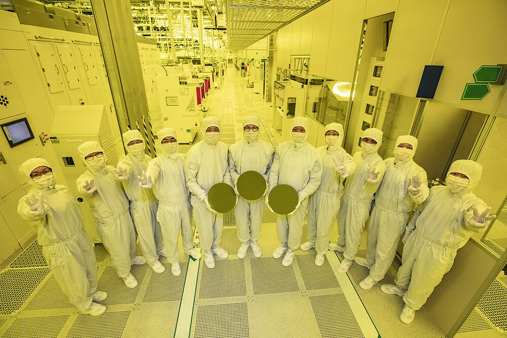
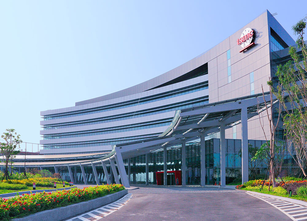
TSMC Celebrates 30th North America Technology Symposium with Innovations Powering AI with Silicon Leadership

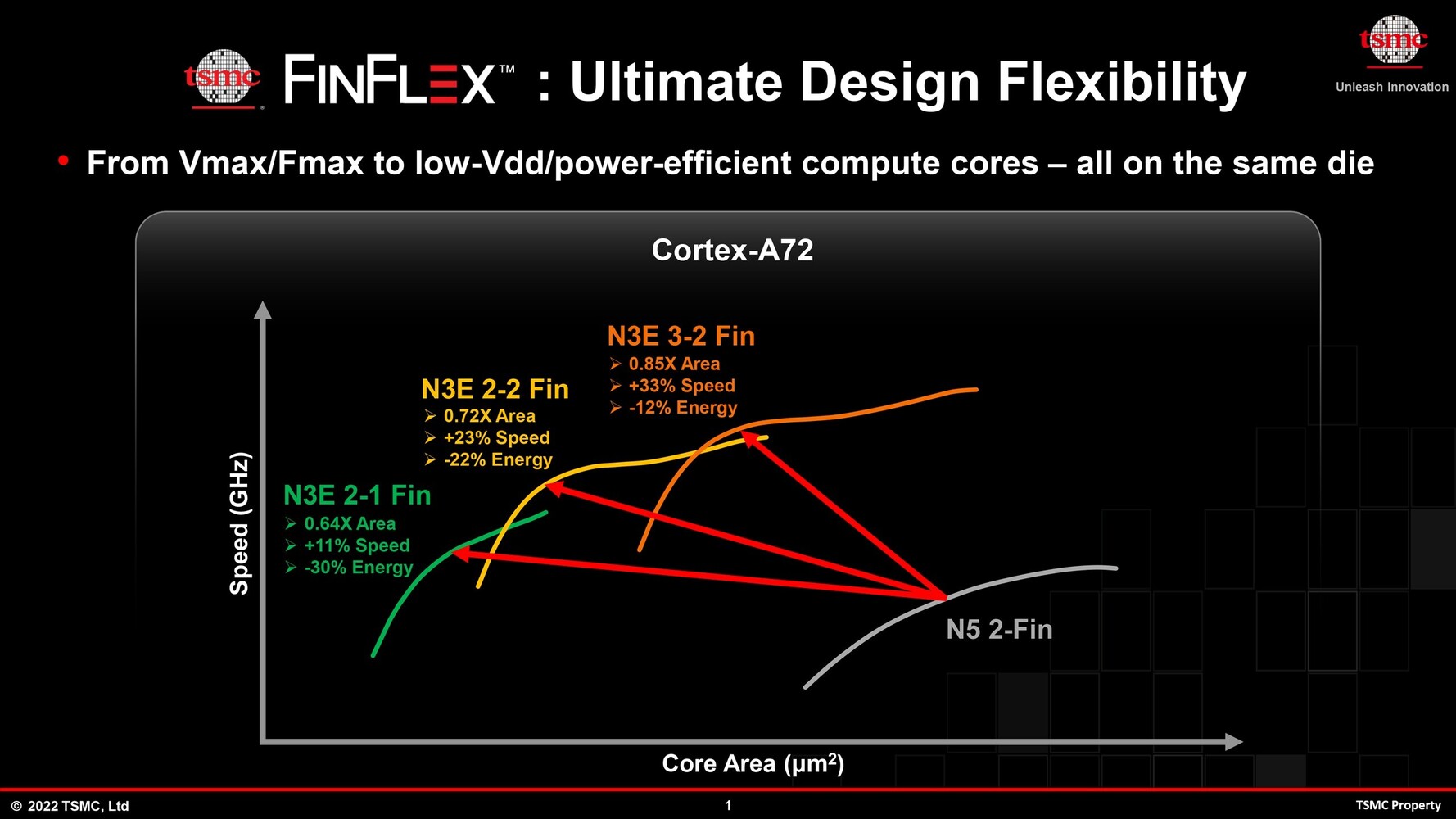
TSMC today unveiled its newest semiconductor process, advanced packaging, and 3D IC technologies for powering the next generation of AI innovations with silicon leadership at the Company's 2024 North America Technology Symposium. TSMC debuted the TSMC A16 technology, featuring leading nanosheet transistors with innovative backside power rail solution for production in 2026, bringing greatly improved logic density and performance. TSMC also introduced its System-on-Wafer (TSMC-SoW) technology, an innovative solution to bring revolutionary performance to the wafer level in addressing the future AI requirements for hyperscaler datacenters.

This year marks the 30th anniversary of TSMC's North America Technology Symposium, and more than 2,000 attended the event, growing from less than 100 attendees 30 years ago. The North America Technology Symposium in Santa Clara, California kicks off TSMC Technology Symposiums around the world in the coming months. The symposium also features an "Innovation Zone," designed to highlight the technology achievements of our emerging start-up customers.

Apple M3 Ultra Chip Could be a Monolithic Design Without UltraFusion Interconnect

As we witness Apple's generational updates of the M series of chips, the highly anticipated SKU of the 3rd generation of Apple M series yet-to-be-announced top-of-the-line M3 Ultra chip is growing speculations from industry insiders. The latest round of reports suggests that the M3 Ultra might step away from its predecessor's design, potentially adopting a monolithic architecture without the UltraFusion interconnect technology. In the past, Apple has relied on a dual-chip design for its Ultra variants, using the UltraFusion interconnect to combine two M series Max chips. For example, the second generation M Ultra chip, M2 Ultra, boasts 134 billion transistors across two 510 mm² chips. However, die-shots of the M3 Max have sparked discussions about the absence of dedicated chip space for the UltraFusion interconnect.

While the absence of visible interconnect space on early die-shots is not conclusive evidence, as seen with the M1 Max not having visible UltraFusion interconnect and still being a part of M1 Ultra with UltraFusion, industry has led the speculation that the M3 Ultra may indeed feature a monolithic design. Considering that the M3 Max has 92 billion transistors and is estimated to have a die size between 600 and 700 mm², going Ultra with these chips may be pushing the manufacturing limit. Considering the maximum die size limit of 848 mm² for the TSMC N3B process used by Apple, there may not be sufficient space for a dual-chip M3 Ultra design. The potential shift to a monolithic design for the M3 Ultra raises questions about how Apple will scale the chip's performance without the UltraFusion interconnect. Competing solutions, such as NVIDIA's Blackwell GPU, use a high-bandwidth C2C interface to connect two 104 billion transistor chips, achieving a bandwidth of 10 TB/s. In comparison, the M2 Ultra's UltraFusion interconnect provided a bandwidth of 2.5 TB/s.

Intel CEO Discloses TSMC Production Details: N3 for Arrow Lake & N3B for Lunar Lake

Intel CEO Pat Gelsinger engaged with press/media representatives following the conclusion of his IFS Direct Connect 2024 keynote speech—when asked about Team Blue's ongoing relationship with TSMC, he confirmed that their manufacturing agreement has advanced from "5 nm to 3 nm." According to a China Times news article: "Gelsinger also confirmed the expansion of orders to TSMC, confirming that TSMC will hold orders for Intel's Arrow and Lunar Lake CPU, GPU, and NPU chips this year, and will produce them using the N3B process, officially ushering in the Intel notebook platform that the outside world has been waiting for many years." Past leaks have indicated that Intel's Arrow Lake processor family will have CPU tiles based on their in-house 20A process, while TSMC takes care of the GPU tile aspect with their 3 nm N3 process node.

That generation is expected to launch later this year—the now "officially confirmed" upgrade to 3 nm should produce pleasing performance and efficiency improvements. The current crop of Core Ultra "Meteor Lake" mobile processors has struggled with the latter, especially when compared to rivals. Lunar Lake is marked down for a 2025 launch window, so some aspects of its internal workings remain a mystery—Gelsinger has confirmed that TSMC's N3B is in the picture, but no official source has disclosed their in-house manufacturing choice(s) for LNL chips. Wccftech believes that Lunar Lake will: "utilize the same P-Core (Lion Cove) and brand-new E-Core (Skymont) core architecture which are expected to be fabricated on the 20A node. But that might also be limited to the CPU tile. The GPU tile will be a significant upgrade over the Meteor Lake and Arrow Lake CPUs since Lunar Lake ditches Alchemist and goes for the next-gen graphics architecture codenamed "Battlemage" (AKA Xe2-LPG)." Late January whispers pointed to Intel and TSMC partnering up on a 2 nanometer process for the "Nova Lake" processor generation—perhaps a very distant prospect (2026).

TSMC 2 nm Node to Debut in 2025 with Apple SoCs for the iPhone 17 Pro

TSMC's 2 nm-class foundry node, dubbed N2, will enter mass production only in 2025, a report by the Financial Times says. The premier Taiwan-based foundry has been reportedly showcasing TSMC N2 to its biggest customer for advanced nodes, Apple. The node will likely power Apple's in-house silicon that drives the iPhone 17 Pro and Pro Max devices that are slated for 2025. This implies that the current 3 nm class nodes from TSMC will continue to power Apple silicon into 2024 and its iPhone 16 Pro/Pro Max.

The current Apple A17 Pro and M3 chips powering the iPhone 15 Pro/Max and the H2-2023 Macs are based on TSMC's N3 node, with a 183 MTr/mm² transistor density. TSMC has four other 3 nm-class nodes, with the N3E node that just entered mass production to offer a jump to 215.6 MTr/mm², and its 2024 successor, the N3P, pushing transistor densities further up to 224 MTr/mm². TSMC's first 2 nm-class node, the N2, offers a jump to around 259 MTr/mm², which makes the N3P a nice halfway point for Apple between the N3 and N2, for its 2024 silicon.

Samsung and TSMC Reportedly Struggling with 3 nm Yields

According to Korean business news publication ChosunBiz, both Samsung and TSMC are struggling with their 3 nm node yields. The two companies have different approaches to their 3 nm nodes, with Samsung using GAA FET (Gate All Around), whereas TSMC is continuing with its FinFET technology. That said, TSMC has at least five known 3 nm nodes, of which two should be in production by now, assuming N3E has proved to be reliable enough to kick off. Samsung on the other hand has three known 3 nm nodes, with only one in production so far, called 3GAE.

ChosunBiz reports that neither company is getting the kind of yields that you'd expect from a node that should have been in volume production for around a year by now, with Samsung apparently being somewhat better than TSMC. At 60 and 50 percent respectively, neither Samsung nor TSMC are anywhere near decent yields. Anything below 70 percent is considered very poor and even the 60 percent claim in Samsungs case, is apparently limited to some kind of Chinese mining ASIC and doesn't include the SRAM you find in most modern processors. ChosunBiz also mentions a source familiar with Samsung's foundry business who mentions a yield closer to 50 percent for the company. The same source also mentions that Samsung needs to reach at least 70 percent yield to be able to attract major customers to its 3 nm node.

Synopsys and TSMC Streamline Multi-Die System Complexity with Unified Exploration-to-Signoff Platform and Proven UCIe IP on TSMC N3E Process

Synopsys, Inc. today announced it is extending its collaboration with TSMC to advance multi-die system designs with a comprehensive solution supporting the latest 3Dblox 2.0 standard and TSMC's 3DFabric technologies. The Synopsys Multi-Die System solution includes 3DIC Compiler, a unified exploration-to-signoff platform that delivers the highest levels of design efficiency for capacity and performance. In addition, Synopsys has achieved first-pass silicon success of its Universal Chiplet Interconnect Express (UCIe) IP on TSMC's leading N3E process for seamless die-to-die connectivity.

"TSMC has been working closely with Synopsys to deliver differentiated solutions that address designers' most complex challenges from early architecture to manufacturing," said Dan Kochpatcharin, head of the Design Infrastructure Management Division at TSMC. "Our long history of collaboration with Synopsys benefits our mutual customers with optimized solutions for performance and power efficiency to help them address multi-die system design requirements for high-performance computing, data center, and automotive applications."

TSMC N3 Nodes Show SRAM Scaling is Hitting the Wall

When TSMC introduced its N3 lineup of nodes, the company only talked about the logic scaling of the two new semiconductor manufacturing steps. However, it turns out that there was a reason for it, as WikiChip confirms that the SRAM bit cells of N3 nodes are almost identical to the SRAM bit cells of N5 nodes. At TSMC 2023 Technology Symposium, TSMC presented additional details about its N3 node lineup, including logic and SRAM density. For starters, the N3 node is TSMC's "3 nm" node family that has two products: a Base N3 node (N3B) and an Enhanced N3 node (N3E). The base N3B uses a new (for TSMC) self-aligned contact (SAC) scheme that Intel introduced back in 2011 with a 22 nm node, which improves the node's yield.

Regardless of N3's logic density improvements compared to the "last-generation" N5, the SRAM density is almost identical. Initially, TSMC claimed N3B SRAM density was 1.2x over the N5 process. However, recent information shows that the actual SRAM density is merely a 5% difference. With SRAM taking a large portion of the transistor and area budget of a processor, N3B's soaring manufacturing costs are harder to justify when there is almost no area improvement. For some time, SRAM scaling wasn't following logic scaling; however, the two have now completely decoupled.

Arm Launches the Cortex-X4, A720 and A520, Immortalis-G715 GPU

Mobile devices touch every aspect of our digital lives. In the palm of your hand is the ability to both create and consume increasingly immersive, AI-accelerated experiences that continue to drive the need for more compute. Arm is at the heart of many of these, bringing unlimited delight, productivity and success to more people than ever. Every year we build foundational platforms designed to meet these increasing compute demands, with a relentless focus on high performance and efficiency. Working closely with our broader ecosystem, we're delivering the performance, efficiency and intelligence needed on every generation of consumer device to expand our digital lifestyles.

Today we are announcing Arm Total Compute Solutions 2023 (TCS23), which will be the platform for mobile computing, offering our best ever premium solution for smartphones. TCS23 delivers a complete package of the latest IP designed and optimized for specific workloads to work seamlessly together as a complete system. This includes a new world-class Arm Immortalis GPU based on our brand-new 5th Generation GPU architecture for ultimate visual experiences, a new cluster of Armv9 CPUs that continue our performance leadership for next-gen artificial intelligence (AI), and new enhancements to deliver more accessible software for the millions of Arm developers.

TSMC Certifies Ansys Multiphysics Solutions for TSMC's N2 Silicon Process

Ansys and TSMC continue their long-standing technology collaboration to announce the certification of Ansys' power integrity software for TSMC's N2 process technology. The TSMC N2 process, which adopts nanosheet transistor structure, represents a major advancement in semiconductor technology with significant speed and power advantages for high performance computing (HPC), mobile chips, and 3D-IC chiplets. Both Ansys RedHawk-SC and Ansys Totem are certified for power integrity signoff on N2, including the effects of self-heat on long-term reliability of wires and transistors. This latest collaboration builds on the recent certification of the Ansys platform for TSMC's N4 and N3E FinFLEX processes.

"TSMC works closely with our Open Innovation Platform (OIP) ecosystem partners to help our mutual customers achieve the best design results with the full stack of design solutions on TSMC's most advanced N2 process," said Dan Kochpatcharin, head of the Design Infrastructure Management Division at TSMC. "Our latest collaboration with Ansys RedHawk-SC and Totem analysis tools allows our customers to benefit from the significant power and performance improvements of our N2 technology while ensuring predictively accurate power and thermal signoff for the long-term reliability of their designs."

TSMC Showcases New Technology Developments at 2023 Technology Symposium

TSMC today showcased its latest technology developments at its 2023 North America Technology Symposium, including progress in 2 nm technology and new members of its industry-leading 3 nm technology family, offering a range of processes tuned to meet diverse customer demands. These include N3P, an enhanced 3 nm process for better power, performance and density, N3X, a process tailored for high performance computing (HPC) applications, and N3AE, enabling early start of automotive applications on the most advanced silicon technology.

With more than 1,600 customers and partners registered to attend, the North America Technology Symposium in Santa Clara, California is the first of the TSMC's Technology Symposiums around the world in the coming months. The North America symposium also features an Innovation Zone spotlighting the exciting technologies of 18 emerging start-up customers.

Synopsys, TSMC and Ansys Strengthen Ecosystem Collaboration to Advance Multi-Die Systems

Accelerating the integration of heterogeneous dies to enable the next level of system scalability and functionality, Synopsys, Inc. (Nasdaq: SNPS) has strengthened its collaboration with TSMC and Ansys for multi-die system design and manufacturing. Synopsys provides the industry's most comprehensive EDA and IP solutions for multi-die systems on TSMC's advanced 7 nm, 5 nm and 3 nm process technologies with support for TSMC 3DFabric technologies and 3Dblox standard. The integration of Synopsys implementation and signoff solutions and Ansys multi-physics analysis technology on TSMC processes allows designers to tackle the biggest challenges of multi-die systems, from early exploration to architecture design with signoff power, signal and thermal integrity analysis.

"Multi-die systems provide a way forward to achieve reduced power and area and higher performance, opening the door to a new era of innovation at the system-level," said Dan Kochpatcharin, head of Design Infrastructure Management Division at TSMC. "Our long-standing collaboration with Open Innovation Platform (OIP) ecosystem partners like Synopsys and Ansys gives mutual customers a faster path to multi-die system success through a full spectrum of best-in-class EDA and IP solutions optimized for our most advanced technologies."

Snapdragon 8 Gen 3 GPU Could be 50% More Powerful Than Current Gen Adreno 740

An online tipster, posting on the Chinese blog site Weibo, has let slip that Qualcomm's upcoming Snapdragon 8 Gen 3 mobile chipset is touted to pack some hefty graphical capabilities. The suggested Adreno "750" smartphone and tablet GPU is touted to offer a 50% increase over the present generation Adreno 740 - as featured on the recently released and cutting-edge Snapdragon 8 Gen 2 chipset. The current generation top-of-the-range Snapdragon is no slouch when it comes to graphics benchmarks, where it outperforms Apple's prime contender - the Bionic A16 SoC.

The Snapdragon 8 Gen 3 SoC is expected to launch in the last quarter of 2023, but details of the flagship devices that it will power are non-existent at the time of writing. The tipster suggests that Qualcomm has decided to remain on TSMC's 4 nm process for its next generation mobile chipset - perhaps an all too safe decision when you consider that Apple has upped the stakes with the approach of its Bionic A17 SoC. It has been reported that the Cupertino, California-based company has chosen to fabricate via TSMC's 3 nm process, although the Taiwanese foundry is said to be struggling with its N3 production line. The engineers at Qualcomm's San Diego headquarters are alleged to be experimenting with increased clock speeds running on the next gen Adreno GPU - as high as 1.0 GHz - in order to eke out as much performance as possible, in anticipation of besting the Bionic A17 in graphics benchmarks. The tipster theorizes that Qualcomm will still have a hard time matching Apple in terms of pure CPU throughput, so the consolation prize will lie with a superior GPU getting rigged onto the Snapdragon 8 Gen 3.

TSMC's 3 nm Node at Near 50 Percent Utilisation, Other Nodes Seeing Lower Demand

Based on multiple reports out of Taiwan, TSMC is seeing increased utilisation of its 3 nm node and its production line is now at close to 50 percent utilisation. The main customer here is without a doubt Apple and TSMC is churning out some 50-55,000 wafers a month on its 3 nm node. TSMC is also getting ready to start production on its N3E node later this year, which will see some customers move to the node.

However, it's not all good news, as TSMC is seeing a decline in utilisation on its 5/4 and 7/6 nm nodes as demand has dropped significantly here, with different news outlets reporting different figures. Some are suggesting the 7/6 nm nodes might have dropped as low as to 50 percent utilisation, others mention 70 percent. The 5/4 nm nodes aren't anywhere nearly as badly affected and remain at around 80 percent utilisation. The good news for TSMC is that this is expected to be a temporary slump in demand and most of its leading edge nodes should be back at somewhere around a 90 percent utilisation rate by the second half of the year. However, this depends on what the demand for its partners' products will look like going forward, as many of TSMC's customers are seeing lower demand for their products in turn.

Intel Defers 3 nm Wafer Orders with TSMC, Pushes "Arrow Lake" Rollout to 2025?

Intel has reportedly deferred its orders for 3 nm wafers with TSMC, sources in PC makers tell Taiwan-based industry observer DigiTimes. Built on the TSMC N3 node, the wafers were supposed to power the Graphics tiles (containing the iGPU), of the upcoming "Arrow Lake" processors, which were originally on course for a 2024 release. The DigiTimes report detailing this development says that Intel's 3 nm wafer orders have been deferred to Q4-2024, which would realistically mean a 2025 launch for whatever product was designed to use 3 nm tiles. Advance orders for next-gen wafers by high-volume clients such as Intel, are usually placed several quarters in advance, so the foundry could suitably scale up its capacity.

TSMC Holds 3nm Volume Production and Capacity Expansion Ceremony, Marking a Key Milestone for Advanced Manufacturing

TSMC today held a 3 nanometer (3 nm) Volume Production and Capacity Expansion Ceremony at its Fab 18 new construction site in the Southern Taiwan Science Park (STSP), bringing together suppliers, construction partners, central and local government, the Taiwan Semiconductor Industry Association, and members of academia to witness an important milestone in the Company's advanced manufacturing.

TSMC has laid a strong foundation for 3 nm technology and capacity expansion, with Fab 18 located in the STSP serving as the Company's GIGAFAB facility producing 5 nm and 3 nm process technology. Today, TSMC announced that 3 nm technology has successfully entered volume production with good yields, and held a topping ceremony for its Fab 18 Phase 8 facility. TSMC estimates that 3 nm technology will create end products with a market value of US$1.5 trillion within five years of volume production.

TSMC to Mark 3 nm Mass Production Start, Looking at Potential New Fabs in Japan and Germany

According to news out of Taiwan, TSMC will hold a ceremony to mark the official mass production start of its 3 nm node on the 29th of December. This is said to help "shatter doubts about de-Taiwanization" or in simpler terms, that Taiwan will lose its golden goose as TSMC invests abroad. The 3 nm fab—known as fab 18—is based in southern Taiwan's Tainan and the ceremony also marks the start of an expansion of TSMC's most advanced fab. TSMC is said to be kicking off its N3E node production sometime in the second half of 2023, followed by its N3P node in 2024, all of which should take place at fab 18, which also produces 5 nm wafers.

In related news, according to Reuters, a Japanese lawmaker from the ruling party has said that TSMC is considering a second plant in Japan, in addition to its current joint venture that is already under construction. TSMC's response to Reuters was that the company isn't ruling out Japan for future fabs, but that the company doesn't have any current plans. At the same time, TSMC is said to be sending executives to Dresden, Germany in early 2023, for a second round of talks about building a fab to help support the European auto industry, although this would be a 28/22 nm fab, which is far from cutting edge these days, although a lot more advanced than most fabs making chips for the auto industry.

TSMC's Morris Chang Says Arizona Fab Will Produce 3 nm Chips in the Future

Although Morris Chang is no longer in charge of the day to day business at TSMC, the founder of the company is still getting his hands dirty. Chang attended the APEC Economic Leaders Meeting last week, as part of Taiwan's delegation and was questioned by the media about TSMC's future plans. The specific question was about TSMC's Arizona fab, which will initially produce chips using a 5 nm node. The US$12 billion plant is scheduled to kick off production at some point in 2024, by which time the 5 nm node should be a commonly used node rather than close to cutting edge.

When questioned about the future of the Arizona fab, Morris Chang answered that it will be moving to a 3 nm node, which is currently TSMC's most cutting edge node, that has gone into volume production earlier this year with th N3 node, which is set to be followed by the N3E node. According to Chang, there's interest by several countries to have TSMC set up fabs there, but apparently this is not something TSMC is considering at the moment. One potential reason for this would be a suitable labour force, something that has already proven to be tough for the Arizona fab.

Alphawave IP Achieves Its First Testchip Tapeout for TSMC N3E Process

Alphawave IP (LSE: AWE), a global leader in high-speed connectivity for the world's technology infrastructure, today announced the successful tapeout of its ZeusCORE100 1-112 Gbps NRZ/PAM4 Serialiser-Deserialiser ("SerDes"), Alphawave's first testchip on TSMC's most advanced N3E process. Alphawave IP will be exhibiting this new product alongside its complete portfolio of high-performance IP, chiplet, and custom silicon solutions at the TSMC OIP Forum on October 26 in Santa Clara, CA as the Platinum sponsor.

ZeusCORE100 is Alphawave's most advanced multi-standard-SerDes, supporting extra-long channels over 45dB and the most requested standards such as 800G Ethernet, OIF 112G-CEI, PCIe GEN6, and CXL 3.0. Attendees will be able to visit the Alphawave booth and meet the company's technology experts including members of the recently acquired OpenFive team. OpenFive is a longstanding partner of TSMC through the OIP Value Chain Aggregator (VCA) program. OpenFive is one of a select few companies with an idea-to-silicon methodology in TSMC's latest technologies, and advanced packaging capabilities, enabling access to the most advanced foundry solution available with the best Power-Performance-Area (PPA). With Alphawave's industry-leading IP portfolio and the addition of OpenFive's capabilities, designers can create systems on a chip (SoCs) that pack more compute power into smaller form factors for networking, AI, storage, and high-performance computing (HPC) applications.

TSMC Cuts Back CAPEX Budget Despite Record Profits

Another quarter, another record breaking earnings report by TSMC, but it seems like the company has released that things are set to slow down sooner than initially expected and the company is hitting the brakes on some of its expansion projects. The company saw a 79.7 percent increase in profits compared to last year, with a profit of US$8.8 billion and a revenue of somewhere between US$19.9 to US$ 20.7 billion for the third quarter, which is a 47.9 percent bump compared to last year. TSMC's 5 nm nodes were the source for 28 percent of the revenues, followed by 26 percent for 7 nm nodes, 12 percent for 16 nm and 10 percent for 28 nm, with remaining nodes at 40 nm and larger making up for the remainder of the revenue. By platform, smartphone chips made up 41 percent, followed by High Performance Computing at 39 percent, IoT at 10 percent and automotive at five percent.

TSMC said it will cut back its CAPEX budget by around US$4 billion, to US$36 billion, compared to the earlier stated US$40 billion budget the company had set aside for expanding its fabs. Part of the reason for this is that TSMC is already seeing weaker demand for products manufactured using its N7 and N6 nodes, as the N7 node was meant to be a key part of the new fab in Kaohsiung in southern Taiwan. TSMC is expecting to start production on its first N3 node later this quarter and is expecting the capacity to be fully utilised for all of 2023. Supply is said to be exceeding demand, which TSMC said is partially to blame on tooling delivery issues. TSMC is expecting next year's revenue for its N3 node to be higher than its N5 node in 2020, although the revenue is said to be in the single digit percentage range. The N3E node is said to start production sometime in the second half of next year, or about a quarter earlier than expected. The N2 node isn't due to start production until 2025, but TSMC is already having very high customer engagement, so it doesn't look like TSMC is likely to suffer from a lack of business in the foreseeable future, as long as the company keeps delivering new nodes as planned.

AMD's CEO Lisa Su Planning Trip to Taiwan, Said to be Visiting TSMC to Secure Future Wafer Allocation

Based on a report by Tom's Hardware, AMD's CEO Lisa Su is planning a trip to Taiwan in the next couple of months. It is said that she is planning to meet with multiple partners in Taiwan, such as ASUS, Acer and maybe more importantly, ASMedia, which will be the sole maker of chipsets for AMD, once the X570 chipset is discontinued. AMD is apparently also seeing various less well known partners that deliver parts for its CPUs, such as Nan Ya PCB, Unimicron Technologies and Kinsus Interconnects.

However, it appears that the main reason for Lisa Su herself to visit Taiwan will be to meet with TSMC, to discuss future collaboration with CC Wei, TSMC's chief executive. This is so AMD can secure enough wafer allocation on future nodes, such as its 3 nm and 2 nm class nodes. The move to these nodes is obviously not happening in the near future for AMD, but considering that TSMC is currently the leading foundry and is operating at capacity, it makes sense to get in early, as the competition is stiff when it comes to getting wafer allocation on cutting edge nodes. It's unclear which exact 3 nm class node AMD will be aiming for, but it might be the N3P node, which is said to kick off production sometime next year. Lisa Su is also said to have meetings with TSMC, SPIL and Ase Technology when it comes to advanced packaging for AMD's products. This includes technologies such as chip-on-wafer-on-substrate (CoWoS) and fan-out embedded bridge (FO-EB), with AMD already being expected to use some of these technologies in its upcoming Navi 3x GPUs.

TSMC has Seven Major Customers Lined Up for its 3 nm Node

Based on media reports out of Taiwan, TSMC seems to have plenty of customers lined up for its 3 nm node, with Apple being the first customer out the gates when production starts sometime next month. However, TSMC is only expected to start the production with a mere 1,000 wafer starts a month, which seems like a very low figure, especially as this is said to remain unchanged through all of Q4. On the plus side, yields are expected to be better than the initial 5 nm node yields. Full-on mass production for the 3 nm node isn't expected to happen until the second half of 2023 and TSMC will also kick off its N3E node sometime in 2023.

Apart from Apple, major customers for the 3 nm node include AMD, Broadcom, Intel, MediaTek, NVIDIA and Qualcomm. Contrary to earlier reports by TrendForce, it appears that TSMC will continue its rollout of the 3 nm node as previously planned. Apple is expected to produce the A17 smartphone and tablet SoC, as well as advanced versions of the M2, as well as the M3 laptop and desktop processors on the 3 nm node. Intel is still said to be producing its graphics chiplets with TSMC, with the potential for GPU and FPGA products in the future. There's no word on what the other customers are planning to produce on the 3 nm node, but MediaTek and Qualcomm are obviously looking at using the node for future smartphone and tablet SoCs, with AMD and NVIDIA most likely aiming for upcoming GPUs and Broadcom for some kind of HPC related hardware.

TSMC Announces the N3 FinFlex, N3E, and N2 Nodes, and 3DFabric

TSMC today showcased the newest innovations in its advanced logic, specialty, and 3D IC technologies at the Company's 2022 North America Technology Symposium, with the next-generation leading-edge N2 process powered by nanosheet transistors and the unique FINFLEX technology for the N3 and N3E processes making their debut.

Resuming as an in-person event after being held online in the past two years, the North America symposium in Santa Clara, California, kicks off a series of Technology Symposiums around the world in the coming months. The Symposiums also feature an Innovation Zone that spotlights the achievements of TSMC's emerging start-up customers.

Cadence Digital and Custom/Analog Design Flows Certified by TSMC for Latest N3E and N4P Processes

Cadence Design Systems, Inc. today announced that its digital and custom/analog design flows have been certified for the TSMC N3E and N4P processes, supporting the latest Design Rule Manual (DRM). In addition, Cadence and TSMC delivered N3E and N4P process design kits (PDKs) and design flows to accelerate customer adoption and advance mobile, AI and hyperscale computing design innovation. Joint customers are actively designing with the new N3E and N4P PDKs, and several test chips have already been taped out, which demonstrates how Cadence solutions help customers improve engineering efficiency and maximize the power, performance and area (PPA) benefits offered by the latest TSMC process technologies. The Cadence digital and custom/analog advanced-node solutions support the company's Intelligent System Design strategy, enabling system-on-chip (SoC) design excellence.

Cadence worked closely with TSMC to ensure the digital full flow was optimized for TSMC's advanced N3E and N4P process technologies. The complete RTL-to-GDS flow includes the Cadence Innovus Implementation System, Quantus Extraction Solution, Quantus Field Solver, Tempus Timing Signoff Solution and ECO option, Pegasus Verification System, Liberate Characterization Solution and Voltus IC Power Integrity Solution. Additionally, the Cadence Genus Synthesis Solution and predictive iSpatial technology are enabled for the TSMC N3E and N4P process technologies.

Intel "Meteor Lake" 2P+8E Silicon Annotated

Le Comptoir du Hardware scored a die-shot of a 2P+8E core variant of the "Meteor Lake" compute tile, and Locuza annotated it. "Meteor Lake" will be Intel's first processor to implement the company's IDM 2.0 strategy to the fullest. The processor is a multi-chip module of various tiles (chiplets), each with a certain function, sitting on die made on a silicon fabrication node most suitable to that function. Under this strategy, for example, if Intel's chip-designers calculate that the iGPU will be the most power-hungry component on the processor, followed by the CPU cores, the graphics tile will be built on a more advanced process than the compute tile. Intel's "Meteor Lake" and "Arrow Lake" processors will implement chiplets built on the Intel 4, TSMC N3, and Intel 20A fabrication nodes, each with unique power and transistor-density characteristics. Learn more about the "Meteor Lake" MCM in our older article.

The 2P+8E (2 performance cores + 8 efficiency cores) compute tile is one among many variants of compute tiles Intel will develop for the various SKUs making up the next-generation Core mobile processor series. The die is annotated with the two large "Redwood Cove" P-cores and their cache slices taking up about 35% of the die area; and the two "Crestmount" E-core clusters (each with 4 E-cores), and their cache slices, taking up the rest. The two P-cores and two E-core clusters are interconnected by a Ring Bus, and share an L3 cache. The size of each L3 cache slice is either 2.5 MB or 3 MB. At 2.5 MB, the total L3 cache will be 10 MB, and at 3 MB, it will be 12 MB. As with all past generations, the L3 cache is fully accessible by all CPU cores in the compute tile.

TSMC First Quarter 2022 Financials Show 45.1% Increase in Revenues

A new quarter and another forecast shattering revenue report from TSMC, as the company beat analysts' forecasts by over US$658 million, with a total revenue for the quarter of US$17.6 billion and a net income of almost US$7.26 billion. That's an increase in net income of 45.1 percent or 35.5 percent in sales. Although the monetary figures might be interesting to some, far more interesting details were also shared, such as production updates about future nodes. As a followup on yesterday's news post about 3 nanometer nodes, the N3 node is officially on track for mass production in the second half of this year. TSMC says that customer engagement is stronger than at the start of its N7 and N7 nodes, with HPC and smartphone chip makers lining up to get onboard. The N3E node is, as reported yesterday, expected to enter mass production in the second half of 2023, or a year after N3. Finally, the N2 node is expected in 2025 and won't adhere to TSMC's two year process technology cadence.

Breaking down the revenue by nodes, N7 has taken back the lead over N5, as N7 accounted for 30 percent of TSMC's Q1 revenues up from 27 percent last quarter, but down from 35 percent in the previous year. N5 sits at 20 percent, which is down from 23 percent in the previous quarter, but up from 14 percent a year ago. The 16 and 28 nm nodes still hold on to 25 percent of TSMC's revenue, which is the same as a year ago and up slightly from the previous quarter. Remaining nodes are unchanged from last quarter.
Return to Keyword Browsing
Apr 25th, 2024 15:46 EDT change timezone

New Forum Posts

Popular Reviews

Controversial News Posts