Wednesday, February 28th 2024

Intel 10A (1 nm-class) Node to Enter Mass Production in 2027

Last week at the Intel Foundry Services Connect event, Intel unveiled its Intel 14A foundry node (1.4 nm-class), to succeed its Intel 18A and Intel 20A nodes, with mass production on this node expected to commence in 2026. It turns out that there is an even more advanced node Intel is working on, which it didn't announce last week, but which was part of an NDA presentation that the company forgot to lift. We're talking about the new Intel 10A node, a 1 nm-class silicon fabrication node that's a generation ahead of Intel 20A. The company says that it expects mass production on the node to begin toward the end of 2027. It is on the backs of these sub-2 nm class nodes, and the impending organizational changes that sees Intel Foundry Services become a more independent commercial entity, that Intel CEO Pat Gelsinger thinks that Intel will become the "TSMC of the West."

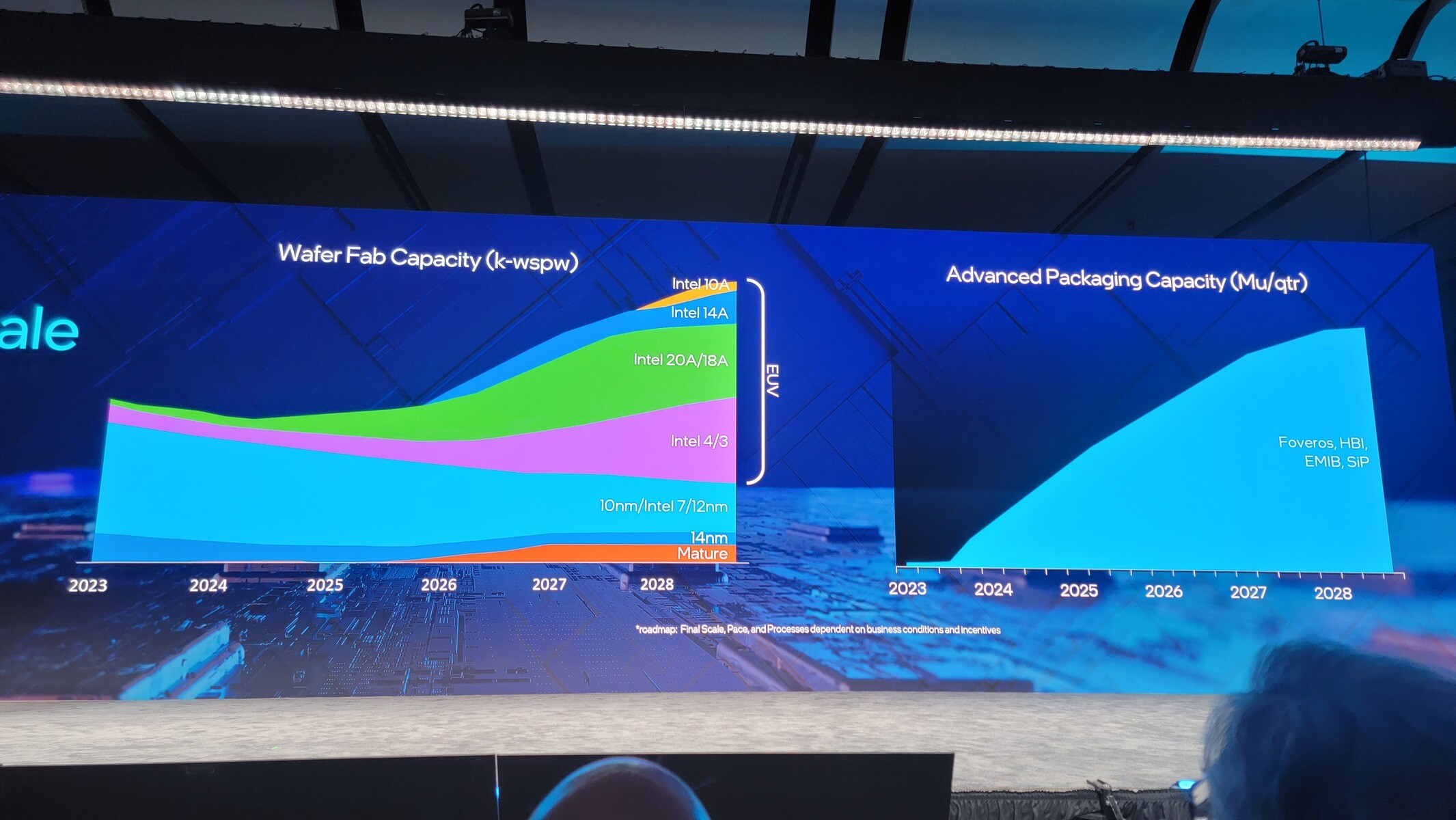
Currently, fabs that utilize EUV (extreme ultraviolet) lithography, namely the Intel 4, Intel 3, and Intel 20A; together make barely 15% of Intel's wafer volumes, with the bulk of the foundry's production focusing on the DUV based Intel 7. EUV-based nodes are expected to linearly grow till 2025, but what's interesting is that Intel doesn't see the kind of multi-year stagnation on Intel 4 and Intel 3 that it's currently experiencing with Intel 7; with wafer volumes of Intel 20A and 18A expected to exceed those of the Intel 4 and Intel 3 within 2025. By 2026, Intel expects that there will be twice as many Intel 20A/18A wafers pushed as Intel 4 and Intel 3. Although they use EUV, Intel 4 and Intel 3 are Intel's final nodes to implement FinFET transistors, as the company transitions to nanosheets with Intel 20A (which are called RibbonFETs in Intel jargon). Intel did not get into the technology behind Intel 10A. The company, along with Samsung and TSMC, demonstrated its stacked CFET transistor in 2023, which will power foundry nodes as nanosheets mature. Intel in its presentation also talked about the next wave of factory automation implemented by IFS, which sees AI-driven "cobots" (collaborative robots) replace humans for more roles in the clean room.
Source: Tom''s Hardware
Add your own comment

40 Comments on Intel 10A (1 nm-class) Node to Enter Mass Production in 2027

#1
Klemc
1nm, and next is 0,xxx.
Posted on Reply
#2
lexluthermiester
Klemc1nm, and next is 0,xxx.
Not for a while. Sub-1nm scales are near atomic scales. It will be some time before methods are found to take advantage of atomic scale circuit manipulation.
Posted on Reply
#4
lexluthermiester
Prima.VeraWhat is 1nm??
1 Nanometer or 1 billionth of a meter.
Posted on Reply
#5
JAB Creations
If this is so great why the rumors that Intel is abandoning their own foundries to use TSMC, drive up demand and therefore the price for AMD? For the clueless, these are rhetorical questions.
Posted on Reply
#6
Daven
lexluthermiesterNot for a while. Sub-1nm scales are near atomic scales. It will be some time before methods are found to take advantage of atomic scale circuit manipulation.
The process is 10A. One nanometer has nothing to do with it. Angstom also has nothing to do with it. Names are mostly marketing now.

Transistor scaling is compared against older planar transistors. With the introduction of FinFet, GAAfet and others, the effective density is given a shrink value compared to how many of these old planar transistors would fit in the same area.

The smallest feature sizes of all competing nodes are still well over 10 nm and nowhere near atomic sizes. Someone posted a good youtube video explaining this a few days ago.

Edit: here it is

Posted on Reply
#7
lexluthermiester
JAB CreationsIf this is so great why the rumors that Intel is abandoning their own foundries to use TSMC
They are not abandoning their existing fabs. They have to use TSMC while they upgrade/rebuild some them to spead out their workload.
DavenThe process is 10A. One nanometer has nothing to do with it. Angstom also has nothing to do with it. Names are mostly marketing now.
Um...
btarunrIntel unveiled its Intel 14A foundry node (1.4 nm-class), to succeed its Intel 18A and Intel 20A nodes
...hmmm.
DavenThe smallest feature sizes are still well over 10 nm and nowhere near atomic sizes. Someone posted a good youtube video explaining this a few days ago.
I am not getting into that pedantic debate..
Posted on Reply
#8
Haku
There is no 1 nm node especially with intel, it's a fake nomenclature
Posted on Reply
#9
Daven
Prima.VeraWhat is 1nm??
Intel renamed its nodes to smaller values to coincide with TSMC even though the process stayed the same. So unless Intel has the power to change length units, you can ignore any ‘nm’ talk. Its just a 10A named process which is smaller than the 14A named process. That’s about all we can say.
Posted on Reply
#10
Klemc
It's 1nm, how they call it, sur thing our eye can't see it !
Posted on Reply
#11
Daven
KlemcIt's 1nm, how they call it, sur thing our eye can't see it !
No company uses ‘nm’ in the naming anymore. Intel names are Intel 4, Intel 3, Intel 20A, etc. TSMC uses N3, N3E, N3X, etc. Samsung uses 3GAE, 3GAP, etc.

And you can ‘see it’ with a scanning electron microscope (SEM) just like you can see the rings of Saturn with a telescope. SEM allows you to measure the smallest feature sizes. Its not magic. Its science.
Posted on Reply
#12
theouto
Hope they actually get there and do it well, we all know that TSMC needs firm competition...
Posted on Reply
#13
Kipicog
JAB CreationsIf this is so great why the rumors that Intel is abandoning their own foundries to use TSMC, drive up demand and therefore the price for AMD? For the clueless, these are rhetorical questions.
Intel uses TSMC for the GPU tile only AFAIK

Intel makes Meteor Lake chips on Intel 4 which is around TSMC 4-5nm in terms of density (hence the name)

Intels 20A factory in germany should be up and running, I guess we will see if Arrow Lake will use 20A or not later this year, might be Intel 4

Also, Intel reserving and taking up space at TSMC is bad for AMD, probably part of the plan too. Apple, Nvidia and now Intel all have priority over AMD at TSMC. AMD always use the older nodes because they are cheaper. Apple always have top priority at TSMC tho. Without Apple, TSMC would not be in the lead. Apple put billions upon billions in TSMCs pockets over the years.

I expect Intel to regain leadership in the coming years tho and they will open up their foundry business. Maybe AMD can get their chips made at Intel LOL
Posted on Reply
#14
Daven
KipicogIntel uses TSMC for the GPU tile only AFAIK

Intel makes Meteor Lake chips on Intel 4 which is around TSMC 4-5nm in terms of density (hence the name)

Intels 20A factory in germany should be up and running, I guess we will see if Arrow Lake will use 20A or not later this year, might be Intel 4

Also, Intel reserving and taking up space at TSMC is bad for AMD, probably part of the plan too. Apple, Nvidia and now Intel all have priority over AMD at TSMC. AMD always use the older nodes because they are cheaper. Apple always have top priority at TSMC tho. Without Apple, TSMC would not be in the lead. Apple put billions upon billions in TSMCs pockets over the years.

I expect Intel to regain leadership in the coming years tho and they will open up their foundry business. Maybe AMD can get their chips made at Intel LOL
It was recently disclosed that Intel is using TSMC for the CPU tile in Arrow Lake and not Intel 20A.

www.techpowerup.com/319517/intel-ceo-discloses-tsmc-production-details-n3-for-arrow-lake-n3b-for-lunar-lake
Posted on Reply
#16
Daven
pressing onI would not read it that way. Intel has officially indicated that the Arrow Lake CPU tile will be on 20A (see graphic below), what the other tiles would be fabricated on was not stated at the time. They are now confirmed as being on TSMC 3nm.

From the TPU article in the link above:

“According to a China Times news article: "Gelsinger also confirmed the expansion of orders to TSMC, confirming that TSMC will hold orders for Intel's Arrow and Lunar Lake CPU, GPU, and NPU chips this year, and will produce them using the N3B process.”

“Past leaks have indicated that Intel's Arrow Lake processor family will have CPU tiles based on their in-house 20A process, while TSMC takes care of the GPU tile aspect with their 3 nm N3 process node.”
Posted on Reply
#17
Klemc
If intel reaches 1nm, so AMD would go fast 0.xxx !!
Posted on Reply
#18
phints
These type of posts are meaningless when Intel HEDT is still many years behind the competion. Apple M3 chips is on TSMC 3nm, AMD Zen 4 is on TSMC 5nm, meanwhile Intel 14th gen using 'Intel 7' node is 5 years behind in lithography and performance per watt. Even if their core design is decent, they simply can't compete being this far behind in lithography.
Posted on Reply
#19
Sabotaged_Enigma
There's recently been a lot of news on Intel process node... but they'd better make it happen rather than talking about it in all kinds of slides.
Posted on Reply
#20
MxPhenom 216
ASIC Engineer
phintsThese type of posts are meaningless when Intel HEDT is still many years behind the competion. Apple M3 chips is on TSMC 3nm, AMD Zen 4 is on TSMC 5nm, meanwhile Intel 14th gen using 'Intel 7' node is 5 years behind in lithography and performance per watt. Even if their core design is decent, they simply can't compete being this far behind in lithography.
Intel will be using the same lithography for sub Intel 7 geometries as TSMC has been using for their 3-7nm. They are not as far behind as you think. Lithography is the technology (ie EUV) used for patterning step of fabricating. Transitioning to EUV is basically mandatory to keep improving density. All major fabs have basically moved to EUV for sub 7nm geos.

For the record, Intel 7 has a smaller fin pitch than TSMC 7 even though its channel length (where traditionally transistors get their sizes) is longer. Intel 7 is also comparable in density as TSMC 7 because the fin pitch is less. Kind of why they call it Intel 7. It used to be their Superfin 10, but recent improvements too it makes it their 7. Its just kind of bad perf/watt.

Basically, saying something is Xnm doesnt mean shit these days due to transistor structures being very different than they used to be and largely marketting now. Transistors can be the same size from say TSMC 7 to TSMC 6, but to make it TSMC 6 they just say its density is improved, perf/watt is better, area better but transistors themselves didnt change. There could even be another flavor of cell that has different VT characteristics added to the library.
Posted on Reply
#21
Wirko
lexluthermiesterI am not getting into that pedantic debate..
Right now, in 2024, it's enough to know the transistors are more than 500 times thinner than a human hair.

But it's not too early for a pedantic debate about what "unveiled" (TPU) or "put on the roadmap" (Tom's) means...

@btarunr The link to Tom's doesn't work, it's truncated by one character.
Posted on Reply
#22
Minus Infinity
So we only know the road map up to end of 2026 for Intel and that ends with Nova Lake using 18A. We don't know what comes in 2027 but that would surely be on 14A and I'm guessing 2028 at earliest for 10A products.
DavenNo company uses ‘nm’ in the naming anymore. Intel names are Intel 4, Intel 3, Intel 20A, etc. TSMC uses N3, N3E, N3X, etc. Samsung uses 3GAE, 3GAP, etc.

And you can ‘see it’ with a scanning electron microscope (SEM) just like you can see the rings of Saturn with a telescope. SEM allows you to measure the smallest feature sizes. Its not magic. Its science.
And yet Samsung and TSMC refer to 3GAE/N3 as 3nm class node. Intel is using A for Angstrom, they could have called their nodes anything and not tried to imply a feature size. All of them are using bogus naming including the likes of ASML.
Posted on Reply
#23
lexluthermiester
WirkoBut it's not too early for a pedantic debate about what "unveiled" (TPU) or "put on the roadmap" (Tom's) means...
I would normally agree with you, It's always a good thing to flesh out information so that minds can be enlightened. However, this particular debate has taken place a number of times and each time ending in the ignorant claiming to have won the debate when in reality they just end up making themselves look like poo-flingers screaming like banshees whilst claiming they had done the same to those arguing factual data and science. This one is not worth the effort as the subject matter is very complex & nuanced and the finer points are often misunderstood or ignored altogether.
Posted on Reply
#24
DavidC1
DavenFrom the TPU article in the link above:

“According to a China Times news article: "Gelsinger also confirmed the expansion of orders to TSMC, confirming that TSMC will hold orders for Intel's Arrow and Lunar Lake CPU, GPU, and NPU chips this year, and will produce them using the N3B process.”

“Past leaks have indicated that Intel's Arrow Lake processor family will have CPU tiles based on their in-house 20A process, while TSMC takes care of the GPU tile aspect with their 3 nm N3 process node.”
Simple. Some are on 20A and some are on N3.
KipicogIntels 20A factory in germany should be up and running, I guess we will see if Arrow Lake will use 20A or not later this year, might be Intel 4
Nothing outside of Meteorlake and the Ericsson SoC is, will be Intel 4. Arrowlake will be 20A and N3 for compute tile.
lexluthermiesterThey are not abandoning their existing fabs. They have to use TSMC while they upgrade/rebuild some them to spead out their workload.
Someone actually using their brain. The whole in-house-or-nothing mentality is hurtful in the short term when they are trying to make sure neither the process team nor the design team gets hampered by delays of each other.
Posted on Reply
#25
Wirko
DavidC1Someone actually using their brain. The whole in-house-or-nothing mentality is hurtful in the short term when they are trying to make sure neither the process team nor the design team gets hampered by delays of each other.
It's also about capacity planning. How many processors are we planning to sell in each quarter of 2025 and 2026? What will our fab capacity be in each quarter? Not enough, just enough or too much?
Posted on Reply
Add your own comment
Apr 29th, 2024 07:11 EDT change timezone

New Forum Posts

Popular Reviews

Controversial News Posts