Thursday, September 10th 2026

Kepler Computing Emerges to Build HBM Alternative Using FeRAM

After seven years of operating in stealth mode, a new startup called Kepler Computing has emerged to address the memory crisis using a custom memory technology. The startup claims to have developed an alternative to HBM using a new 3D stacking technique and novel materials, all without relying on cutting-edge semiconductor nodes. Kepler reportedly plans to use ferroelectric RAM (FeRAM). This use of FeRAM is said to allow Kepler to maintain the standard HBM capacity while significantly reducing manufacturing costs. The company has reportedly overcome many challenges in scaling production and has undergone 35 iterations of composites before settling on a single scalable design.

While modern memory production typically requires EUV lithography, Kepler intends to use existing mature nodes to manufacture HBM and SRAM using FeRAM. In early collaborations with GlobalFoundries, Kepler managed to convert a standard 28 nm manufacturing facility into a memory fab in just eight months, which is significantly faster than the typical 24-month lead time for traditional DRAM. Currently, the company has processed about 2,000 wafers of the new DRAM technology, with the first HBM samples expected to arrive later this year. For full-scale volume manufacturing, the company aims to begin production runs at GlobalFoundries' Singapore facility next year, with manufacturing in the United States slated to start in 2028.
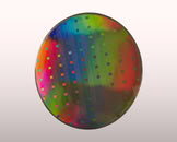
The company has also raised significant funds, securing about $468 million in funding over the past few years from GlobalFoundries, as well as two silicon giants, Intel Capital and AMD Ventures, who are likely to be future customers. Some skepticism remains, as many memory startups have emerged but struggled to achieve yield and technology viability. If Kepler has truly overcome these technical challenges, we hope to see the first HBM-like chips and their density, bandwidth, and other specifications soon.
Source: Wired
Add your own comment

18 Comments on Kepler Computing Emerges to Build HBM Alternative Using FeRAM

#1
Grimling
What will they do with all that DRAM-Capacity that they are building up right now, after the circular financing scam known as the "AI-Bubble" will pop? And that will eventually happen, sooner or later!
Posted on Reply
#2
_JP_
That is fantastic, but it is also just another manufacturing line converted to make HBM, to feed the market that somehow isn't grinding to a halt yet.
I get that FeRAM can be advantageous for HBM, but then free-up the other lines to make DDR5(X) for the rest of us.
Also, haven't heard of GlobalFoundries for a while now. Nice to know those guys are still around and getting contracts.
Posted on Reply
#3
Solid State Brain
_JP_That is fantastic, but it is also just another manufacturing line converted to make HBM, to feed the market that somehow isn't grinding to a halt yet.
If it's so inexpensive, why wouldn't you want FeRAM HBM too?
Posted on Reply
#4
_JP_
Solid State BrainIf it's so inexpensive, why wouldn't you want FeRAM HBM too?
I do...? Do you see any consumer products laying around using HBM?
If I go to the professional/enterprise market, I have plenty of options, but they are also costing considerably for what I would use them for in a personal environment.
Posted on Reply
#5
lambda
Their claims feel overstated. Only time will tell.
Posted on Reply
#6
Solid State Brain
_JP_I do...? Do you see any consumer products laying around using HBM?
There currently aren't, because HBM costs 3-4 times as much to manufacture than equivalent-node DRAM and the enterprise market is eating all the supply, but if manufacturing prices can be slashed (there are many fabs that can produce 28 nm chips), then consumer applications will quickly come.
Posted on Reply
#7
_Under2World_
_JP_I do...? Do you see any consumer products laying around using HBM?
If I go to the professional/enterprise market, I have plenty of options, but they are also costing considerably for what I would use them for in a personal environment.
Even if they're not directly producing consumer product, it will lower the charge on the production capacity that could make consumer product but doesn't because they doing HBM with it.
From what we read they will either create new line or use old one that are underutilized (I don't think the 20-28nm line are running at full capacity right now)
Posted on Reply
#8
BoxCutter
Solid State BrainThere currently aren't, because HBM costs 3-4 times as much to manufacture than equivalent-node DRAM and the enterprise market is eating all the supply, but if manufacturing prices can be slashed (there are many fabs that can produce 28 nm chips), then consumer applications will quickly come.
That's what I wanted to know, what were those nodes even producing?
Posted on Reply
#9
Solid State Brain
BoxCutterThat's what I wanted to know, what were those nodes even producing?
Hard to find a source that explains it clearly and doesn't look AI-generated, but older process nodes are still used for microcontroller units, integrated chips and other low-power applications where having the best possible performance isn't essential. If the chip is not a modern CPU, GPU core, DRAM, or the latest NAND Flash, it's probably been manufactured on a 28nm process node or larger.
Posted on Reply
#10
BoxCutter
Solid State BrainHard to find a source that explains it clearly and doesn't look AI-generated, but older process nodes are still used for microcontroller units, integrated chips and other low-power applications where having the best possible performance isn't essential. If the chip is not a modern CPU, GPU core, DRAM, or the latest NAND Flash, it's probably been manufactured on a 28nm process node or larger.
That's what I thought, that means that's a huge increase in productivity if they managed to use such an old/mature node to make something this valuable, need to actually see how it will play of course. These are just promises as of now.
Posted on Reply
#11
user556
Eek! FRAM as main memory, that's gonna need wear-leveling of some sort.
Posted on Reply
#12
shuffy_losys
user556Eek! FRAM as main memory, that's gonna need wear-leveling of some sort.
FeRAM is basically core memory taken to the logical extreme. There's no wear leveling needed.
Posted on Reply
#13
Frank_100
If their stacking tech is general enough it could be applied to ReRam.
That would be the end of NAND.
Posted on Reply
#14
user556
shuffy_losysFeRAM is basically core memory taken to the logical extreme. There's no wear leveling needed.
That's MRAM.

FRAM is an EEPROM tech, same as Flash memory. It depends on shifting atoms.
Posted on Reply
#15
TheEndIsNear
It's all about the bandwidth. That's why all the ai stuff works. Intel is coming with xhbm soon and their stacking tech is really good. I mean 98% yield on EMIB-T is insane. That's with thru silicon vias that's just insane physics to me.
Posted on Reply
#16
shuffy_losys
user556FRAM is an EEPROM tech, same as Flash memory. It depends on shifting atoms.
And having another look at references, no, it's not. EEPROM uses quantum tunneling as the mechanism to store a charge. FeRAM uses basically a capacitor, just with a material that holds the charge for a much longer period of time.

However, I did find that FeRAM has limited endurance, but it's on the order of 10^15 read-write cycles at the upper end. I'm pretty sure that's well within the "device will be obsolete long before the cells wear out" territory.
Posted on Reply
#17
user556
I used EEPROM as a general classification term. Basically making the distinction between RAMs and ROMs. I guess I should have just said FRAM is a ROM tech.
Posted on Reply
#18
neoOpus
We should care more about price than density, it can be adapted to increase density by stacking more and accepting that it will be even if it is 10x thicker as a chip than the actual chips and that they will be multiplexed or that the data is written in parallel in several chips at a time to reduce latency by adjusting the writing and reading speed to be compensating for what ever it takes every bit to be written or read, by just using parallelism more and more and also we can make them less prone to errors by doubling the storage space and letting every bit to be written in at least two locations with CRC as being part of the process to increase reliability... They must be cheap and they must be power efficient not needing colling preferably by making them radiate better any residual heat via some innovative packaging techniques that would allow stacking at manufacturing levels more layers of these at every chip level but also at the level of the die and having thousands of additional connections between them to solve this problem, so single memory module can be 2-5 cm thick if it it will solve the bottleneck with AI, if it will not require any new technologies to be developed other than what we got so far that dates back to 10 years and that is capable of producing billions of these modules per year. Preferably per month and that will relieve the supply chain by giving options to the markets to go for, and some will decide to go for this because it is even if bulkier and a bit slower and consuming few watts more, it must make sense economically as it will still help making AI more accessible to billions of people and making sure that everyone get few billions of tokens per day for less than 1 usd per day to kickstart the progress and accelerate the problems solving, and it will be paying for itself including the extra consumption of power by solving that at different other. Levels, we don't need to use the SOTA technology in everything, not in a mobile device if it does not make sense to use it, so we keep the EU FABs for the devices that we still need to carry around with us, we use these chips to be as close as possible to the sources of power sources and reduce carbon emissions and losses... And recovery using clever technologies of all eras to help wit the cooling and reuse of wasted heat.
GrimlingWhat will they do with all that DRAM-Capacity that they are building up right now, after the circular financing scam known as the "AI-Bubble" will pop? And that will eventually happen, sooner or later!
Nothing is going yo waste as we should impose them to not destroy any of it like they will usually do, we must be very sever about this this time, we have use for it and via laws we can make them opt to just make the right choice instead of the greed-based choice... They must understand that they will benefit from that as it will be used to make the world better by the global collective and that will give them something back that no amount of money can buy them, as money cannot buy what doesn't exist, yet.
Posted on Reply
Add your own comment
Nov 12th, 2026 04:40 CST change timezone

New Forum Posts

Popular Reviews

TPU on YouTube

Controversial News Posts