Friday, September 25th 2026

TSMC Begins A14 Pilot Production, Risk Production Next Year
TSMC's A14 node, which produces 1.4 nm chips, has reportedly begun pilot production runs at Hsinchu Science Park's Baoshan Fab 20 and Central Taiwan Science Park's Fab 25, where TSMC's latest and most advanced nodes are developed. According to UDN, TSMC is conducting pilot production to evaluate the viability of the semiconductor node, allowing customers to see how their potential designs will perform in TSMC's production environment. This is a positive sign for TSMC, as the A14 node production is progressing better than expected, with timelines moving forward due to early success. If the pilot production proceeds smoothly without major yield or production issues, risk production is scheduled to begin next year in 2027, followed by high-volume manufacturing in 2028. If no significant issues arise next year, TSMC might even advance the production schedule by a few months.
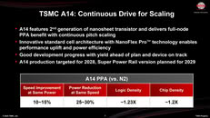
Compared to the recently announced volume production of the N2 2 nm node, the A14 process offers up to 15% higher speeds at the same power level or up to 30% power reduction at the same frequency. TSMC also claims a 20% increase in logic density, with logic components scaling more effectively with larger jumps between nodes, unlike the previous sub-10 nm era. All of this will first be implemented in Taiwan at TSMC's main headquarters, where the company plans to mass-produce the node in 2028. This positions TSMC with a slight time advantage over Samsung and Intel, making it a direct competitor to Intel's 14A in the angstrom era of semiconductor manufacturing.
 A few months ago, we reported that TSMC is allegedly using artificial intelligence and virtual reality to aid in the fab's development. AI is being used for image recognition and smart inspection, while VR simulations assist with training for high-altitude work and potential hazard situations. This combination of rapid training, construction aid, and other innovations is enabling TSMC to deliver the fab ahead of its internal schedules, allowing the A14 node to progress from zero to initial risk production by the end of 2027. Additionally, TSMC will continue to use Low-NA EUV lithography for A14 node, as it only plans to transition to High-NA around 1 nm node.
Source:
UDN
Compared to the recently announced volume production of the N2 2 nm node, the A14 process offers up to 15% higher speeds at the same power level or up to 30% power reduction at the same frequency. TSMC also claims a 20% increase in logic density, with logic components scaling more effectively with larger jumps between nodes, unlike the previous sub-10 nm era. All of this will first be implemented in Taiwan at TSMC's main headquarters, where the company plans to mass-produce the node in 2028. This positions TSMC with a slight time advantage over Samsung and Intel, making it a direct competitor to Intel's 14A in the angstrom era of semiconductor manufacturing.


3 Comments on TSMC Begins A14 Pilot Production, Risk Production Next Year
For Datacenter? They will take any increase in density/reduction in equivalent power consumption.
Rubin is launching on N3P
Otherwise it's just the A20 actually shipping.
N14 / 14A are probably going to show up in PCs ~2030.
IoW, who cares. Let's see how N2 does.