Thursday, April 23rd 2026
TSMC Says Low-NA EUV Will Carry It Further, Delaying High-NA Adoption
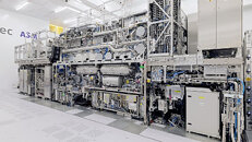
Yesterday, TSMC unveiled its latest A13 node preview at the North America Technology Symposium, highlighting the company's ongoing developments. However, the most significant news isn't about a new node but the technology behind it. TSMC announced it would rely on older ASML Low-NA EUV tools instead of the more expensive High-NA EUV scanners. With the High-NA EUV scanner priced at about €350 million ($410 million), the capital expenditure required to equip a modern facility is substantial. TSMC claims it can maintain a competitive advantage using the existing Low-NA EUV technology, which costs roughly half as much per machine. Kevin Zhang, TSMC's deputy Co-COO and SVP, noted to Reuters, "This is where I think our R&D has done exceptionally well in terms of leveraging existing EUV technology while setting an aggressive technology scaling roadmap. This is definitely a strength."
TSMC's use of Low-NA EUV lithography involves a technique called multi-patterning, where the EUV machine takes multiple passes to etch a design on a single layer. By performing two Low-NA etching runs, TSMC can achieve benefits similar to High-NA exposure, effectively reducing the need for new tools. However, there are limitations to the Low-NA multi-patterning technique, which will be addressed later by introducing High-NA systems, but only for nodes at 1 nm and below. For now, and for recent nodes, TSMC sees a way to maximize performance from the existing Low-NA systems at a much lower capital expenditure than would be required for High-NA systems.
 Interestingly, Intel used a similar tactic during the development of its original, long-delayed 10 nm node. The company initially believed that problems could be solved using traditional DUV machines with multi-patterning techniques, only to find later that the introduction of Low-NA EUV could resolve many of these issues and improve yields. Today, Intel is in the opposite situation, being the first to adopt the High-NA EUV systems, which are more aggressive with etching and are resolving many issues for the 14A node. TSMC now trails in adopting ASML's newest systems, with Intel leading the integration. We hope TSMC doesn't find itself in the same position as Intel due to the more costly equipment and that it can extract more from its current systems. However, at some point, the integration of High-NA EUV lithography will be essential.
Source:
via Reuters
TSMC's use of Low-NA EUV lithography involves a technique called multi-patterning, where the EUV machine takes multiple passes to etch a design on a single layer. By performing two Low-NA etching runs, TSMC can achieve benefits similar to High-NA exposure, effectively reducing the need for new tools. However, there are limitations to the Low-NA multi-patterning technique, which will be addressed later by introducing High-NA systems, but only for nodes at 1 nm and below. For now, and for recent nodes, TSMC sees a way to maximize performance from the existing Low-NA systems at a much lower capital expenditure than would be required for High-NA systems.


4 Comments on TSMC Says Low-NA EUV Will Carry It Further, Delaying High-NA Adoption
Anyhow, stitching will be required to make dies larger than 26 x 16.5 mm. It comes with its own set of issues. Here I might be seeing to far into the future but once stitching is improved enough, it could be employed to make dies larger than the current limit of 26 x 33 mm with more than two exposures.