Tuesday, October 27th 2026
Micron Plans 400-Layer 3D NAND with Wafer-to-Wafer Bonding in 2027
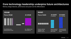
Micron is actively working on bringing its next-generation G11 NAND Flash technology to production, as the company has announced that G11 will be its first 3D NAND Flash. With the current G9 technology shipping across Micron's product portfolio, the company has created NAND Flash storage modules using over 200 layers of scaling. However, as the current technology reaches its limitations, the next phase involves exploring vertical stacking. With G11, Micron aims to use wafer-on-wafer 3D NAND stacking to double the capacity of NAND modules. Micron is now officially following in the footsteps of Chinese NAND giant YMTC, which has been making 3D stacked NAND for some time using Xtacking technology.
This is achieved by splitting each wafer into separate components. One is designed as a memory cell wafer, while the other contains peripheral logic circuits. These are combined using hybrid bonding technology in wafer-to-wafer stacking. Hybrid bonding creates a permanent bond between two silicon chips using embedded metal bumps that fuse together to form a single chip. Multiple dies or entire silicon wafers can be connected by stacking the back ends of two chips together. In this way, Micron plans to ship 400-layer NAND in the second half of 2027, which is less than a year away, and we are about to see more commercialization of 3D silicon.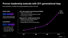
 For capacity and speed, Micron advertises that G11 will double the density per square millimeter. From 21 Gb/mm² for G9, the G11 generation is targeting 42 Gb/mm². Other improvements include a much faster I/O speed, increasing from 3,600 MT/s in G9 to 5,400 MT/s with G11, while efficiency is expected to be significantly improved with 25% lower energy transfer per bit. Real-world performance will depend on the number of these 3D NAND chips in the SSD, as well as the controller, firmware, and interface that the SSD uses to communicate with the host system. Therefore, we don't yet know what kind of speeds consumers can expect, but rest assured, we will be benchmarking them in the future.
Source:
via Tom's Hardware
This is achieved by splitting each wafer into separate components. One is designed as a memory cell wafer, while the other contains peripheral logic circuits. These are combined using hybrid bonding technology in wafer-to-wafer stacking. Hybrid bonding creates a permanent bond between two silicon chips using embedded metal bumps that fuse together to form a single chip. Multiple dies or entire silicon wafers can be connected by stacking the back ends of two chips together. In this way, Micron plans to ship 400-layer NAND in the second half of 2027, which is less than a year away, and we are about to see more commercialization of 3D silicon.


8 Comments on Micron Plans 400-Layer 3D NAND with Wafer-to-Wafer Bonding in 2027
"the company has announced that G11 will be its first 3D NAND Flash"
Er no, G1 was their first 3D NAND Flash, we've had 8 successful generations of 3D NAND Flash from Micron so far, from 32 layers up to 276 layers since G7. Try again, useless Micron marketing goon #4854....