Report an Error


NVIDIA A100X
- Graphics Processor
- GA100
- Cores
- 6912
- TMUs
- 432
- ROPs
- 160
- Memory Size
- 80 GB
- Memory Type
- HBM2e
- Bus Width
- 5120 bit

GPU
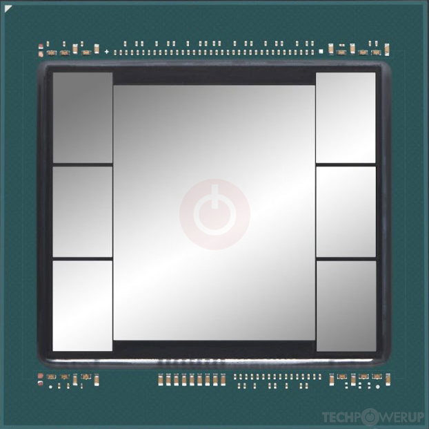
The A100X is a professional graphics card by NVIDIA, launched on June 28th, 2021. Built on the 7 nm process, and based on the GA100 graphics processor, the card does not support DirectX. Since A100X does not support DirectX 11 or DirectX 12, it might not be able to run all the latest games. The GA100 graphics processor is a large chip with a die area of 826 mm² and 54,200 million transistors. It features 6912 shading units, 432 texture mapping units, and 160 ROPs. Also included are 432 tensor cores which help improve the speed of machine learning applications. NVIDIA has paired 80 GB HBM2e memory with the A100X, which are connected using a 5120-bit memory interface. The GPU is operating at a frequency of 795 MHz, which can be boosted up to 1440 MHz, memory is running at 1593 MHz.
Being a dual-slot card, the NVIDIA A100X draws power from 1x 16-pin power connector, with power draw rated at 300 W maximum. This device has no display connectivity, as it is not designed to have monitors connected to it. A100X is connected to the rest of the system using a PCI-Express 4.0 x8 interface. The card measures 267 mm in length, 112 mm in width, and features a dual-slot cooling solution.
Being a dual-slot card, the NVIDIA A100X draws power from 1x 16-pin power connector, with power draw rated at 300 W maximum. This device has no display connectivity, as it is not designed to have monitors connected to it. A100X is connected to the rest of the system using a PCI-Express 4.0 x8 interface. The card measures 267 mm in length, 112 mm in width, and features a dual-slot cooling solution.
Graphics Processor
Graphics Card
- Release Date
- Jun 28th, 2021
- Generation
-
Tesla Ampere
(Axx)
- Predecessor
- Tesla Turing
- Successor
- Tesla Ada
- Production
- Active
- Bus Interface
- PCIe 4.0 x8
Relative Performance
Based on TPU review data: "Performance Summary" at 1920x1080, 4K for 2080 Ti and faster.
Performance estimated based on architecture, shader count and clocks.
Clock Speeds
- Base Clock
- 795 MHz
- Boost Clock
- 1440 MHz
- Memory Clock
-
1593 MHz
3.2 Gbps effective
Memory
- Memory Size
- 80 GB
- Memory Type
- HBM2e
- Memory Bus
- 5120 bit
- Bandwidth
- 2.04 TB/s
Render Config
- Shading Units
- 6912
- TMUs
- 432
- ROPs
- 160
- SM Count
- 108
- Tensor Cores
- 432
- L1 Cache
- 192 KB (per SM)
- L2 Cache
- 80 MB
Theoretical Performance
- Pixel Rate
- 230.4 GPixel/s
- Texture Rate
- 622.1 GTexel/s
- FP16 (half)
- 79.63 TFLOPS (4:1)
- FP32 (float)
- 19.91 TFLOPS
- FP64 (double)
- 9.953 TFLOPS (1:2)
Board Design
- Slot Width
- Dual-slot
- Length
- 267 mm
10.5 inches
- Width
- 112 mm
4.4 inches
- TDP
- 300 W
- Suggested PSU
- 700 W
- Outputs
- No outputs
- Power Connectors
- 1x 16-pin
Graphics Features
- DirectX
- N/A
- OpenGL
- N/A
- OpenCL
- 3.0
- Vulkan
- N/A
- CUDA
- 8.0
- Shader Model
- N/A
GA100 GPU Notes
| Tensor Cores: 3rd Gen NVENC: No Support NVDEC: 4th Gen x5 PureVideo HD: VP10 VDPAU: Feature Set J |
May 4th, 2024 18:29 EDT
change timezone
Latest GPU Drivers
New Forum Posts
- What's your latest tech purchase? (20437)
- RX 6800 causing stuttering when typing text (Low 2D/IDLE Clocks?) (22)
- Battery swap for cyberpower UPS (50)
- NASA Achieves milestone Solid State Battery (226)
- i9-12900K 16 Running Hot (8)
- Change GPU or PSU ? Games looks bad with microsuttering (10)
- Strange system crashes out of nowhere, help (24)
- Alphacool CORE 1 CPU block - bulging with danger of splitting? (94)
- Is updating BIOS to beta versions a good idea if you have the most recent version installed but still face issues? (0)
- AMD RX 7000 series GPU Owners' Club (1098)
Popular Reviews
- Finalmouse UltralightX Review
- Meze Audio LIRIC 2nd Generation Closed-Back Headphones Review
- ASRock NUC BOX-155H (Intel Core Ultra 7 155H) Review
- Montech Sky Two GX Review
- Gigabyte GeForce RTX 4070 Ti Super Gaming OC Review
- Upcoming Hardware Launches 2023 (Updated Feb 2024)
- Cougar Hotrod Royal Gaming Chair Review
- HYTE THICC Q60 240 mm AIO Review
- Alienware Pro Wireless Gaming Keyboard Review
- AMD Ryzen 7 7800X3D Review - The Best Gaming CPU
Controversial News Posts
- Intel Statement on Stability Issues: "Motherboard Makers to Blame" (237)
- Windows 11 Now Officially Adware as Microsoft Embeds Ads in the Start Menu (167)
- AMD to Redesign Ray Tracing Hardware on RDNA 4 (129)
- Sony PlayStation 5 Pro Specifications Confirmed, Console Arrives Before Holidays (117)
- AMD's RDNA 4 GPUs Could Stick with 18 Gbps GDDR6 Memory (114)
- NVIDIA Points Intel Raptor Lake CPU Users to Get Help from Intel Amid System Instability Issues (106)
- AMD "Strix Halo" Zen 5 Mobile Processor Pictured: Chiplet-based, Uses 256-bit LPDDR5X (103)
- AMD Ryzen 9 7900X3D Now at a Mouth-watering $329 (103)