Report an Error
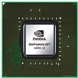
NVIDIA GeForce GT 640M LE
- Graphics Processor
- GK107
- Cores
- 384
- TMUs
- 32
- ROPs
- 16
- Memory Size
- 1024 MB
- Memory Type
- DDR3
- Bus Width
- 128 bit
Recommended Gaming Resolutions:
- 640x480
- 1280x720
- 1366x768
The GeForce GT 640M LE was a mobile graphics chip by NVIDIA, launched on March 22nd, 2012. Built on the 28 nm process, and based on the GK107 graphics processor, in its N13P-LP variant, the chip supports DirectX 12. Even though it supports DirectX 12, the feature level is only 11_0, which can be problematic with newer DirectX 12 titles. The GK107 graphics processor is an average sized chip with a die area of 118 mm² and 1,270 million transistors. It features 384 shading units, 32 texture mapping units, and 16 ROPs. NVIDIA has paired 1,024 MB DDR3 memory with the GeForce GT 640M LE, which are connected using a 128-bit memory interface. The GPU is operating at a frequency of 500 MHz, which can be boosted up to 570 MHz, memory is running at 900 MHz.
Its power draw is rated at 20 W maximum. This device has no display connectivity, as it is not designed to have monitors connected to it. Rather it is intended for use in laptop/notebooks and will use the output of the host mobile device. GeForce GT 640M LE is connected to the rest of the system using a PCI-Express 3.0 x16 interface.
Its power draw is rated at 20 W maximum. This device has no display connectivity, as it is not designed to have monitors connected to it. Rather it is intended for use in laptop/notebooks and will use the output of the host mobile device. GeForce GT 640M LE is connected to the rest of the system using a PCI-Express 3.0 x16 interface.
Graphics Processor
Mobile Graphics
- Release Date
- Mar 22nd, 2012
- Generation
- GeForce 600M
- Predecessor
- GeForce 500M
- Successor
- GeForce 700M
- Production
- End-of-life
- Bus Interface
- PCIe 3.0 x16
- Reviews
- 2 in our database
Relative Performance
Based on TPU review data: "Performance Summary" at 1920x1080, 4K for RTX 3080 and faster.
Performance estimated based on architecture, shader count and clocks.
Clock Speeds
- Base Clock
- 500 MHz
- Boost Clock
- 570 MHz
- Memory Clock
-
900 MHz
1800 Mbps effective
Memory
- Memory Size
- 1024 MB
- Memory Type
- DDR3
- Memory Bus
- 128 bit
- Bandwidth
- 28.80 GB/s
Render Config
- Shading Units
- 384
- TMUs
- 32
- ROPs
- 16
- SMX Count
- 2
- L1 Cache
- 16 KB (per SMX)
- L2 Cache
- 256 KB
Theoretical Performance
- Pixel Rate
- 4.560 GPixel/s
- Texture Rate
- 18.24 GTexel/s
- FP32 (float)
- 437.8 GFLOPS
- FP64 (double)
- 18.24 GFLOPS (1:24)
Board Design
- Slot Width
- IGP
- TDP
- 20 W
- Outputs
- Portable Device Dependent
- Power Connectors
- None
Graphics Features
- DirectX
- 12 (11_0)
- OpenGL
- 4.6
- OpenCL
- 3.0
- Vulkan
- 1.2.175
- CUDA
- 3.0
- Shader Model
- 6.5 (5.1)
Card Notes
| Memory Variant: 2048MB DDR3 Memory Variant: 1024MB GDDR5 |
GK107 GPU Notes
| NVENC: 1st Gen NVDEC: 1st Gen PureVideo HD: VP5 VDPAU: Feature Set D L1 Cache is configurable from 16 KB up to 48 KB per SMX Latest Drivers: Windows XP / Server 2003 x64: Quadro Release R319 U2 (321.01) Windows Vista: GeForce Release 365.19 Quadro Release R346 U7 (348.40) / R352 BETA (352.86) Windows 7 / 8 / 8.1 / 10 / 11 (x32 / x64): GeForce Release 391.35 / 475.06 Quadro Release R390 U9 (392.37) / R470 U16 (474.82) |
Devices based on this design (3)
| Name | GPU Clock | Boost Clock | Memory Clock | Other Changes |
|---|---|---|---|---|
| 624 MHz | 709 MHz | 900 MHz | 2 GB | |
| 500 MHz | 570 MHz | 1000 MHz | GDDR5 | |
| 500 MHz | 570 MHz | 900 MHz | 2 GB |
Aug 2nd, 2025 03:13 CDT
change timezone
Latest GPU Drivers
New Forum Posts
- What's your latest tech purchase? (24429)
- Free Games Thread (4838)
- 3DMARK "LEGENDARY" (359)
- memory used for store firmware in adapters wifi usb (4)
- Samsung 870 EVO - Beware, certain batches prone to failure! (1306)
- What antivirus do you use? (61)
- Laptop WWAN SSD? (4)
- I just bought an RX570 4Gb (27)
- TechPowerUp Screenshot Thread (MASSIVE 56K WARNING) (4285)
- Question about Intel Optane SSDs (90)
Popular Reviews
- ASUS ROG Crosshair X870E Apex Review
- MSI Claw 8 AI+ A2VM Review
- Montech X5 Review
- Orbital Pathfinder Review
- Herman Miller Logitech G Embody Review - No Pain, No Gain
- Lenovo Legion 5i (15IRX10) Review - Feature-Rich and Wallet Friendly
- Lian Li HydroShift II LCD-C 360TL Review
- Upcoming Hardware Launches 2025 (Updated May 2025)
- Noctua NF-A12x25 G2 PWM Fan Review
- Lian Li O11 Dynamic Mini V2 Review
TPU on YouTube
Controversial News Posts
- AMD's Upcoming UDNA / RDNA 5 GPU Could Feature 96 CUs and 384-bit Memory Bus (138)
- AMD Radeon RX 9070 XT Gains 9% Performance at 1440p with Latest Driver, Beats RTX 5070 Ti (131)
- Intel "Nova Lake-S" Core Ultra 3, Ultra 5, Ultra 7, and Ultra 9 Core Configurations Surface (110)
- DDR6 Memory Arrives in 2027 with 8,800-17,600 MT/s Speeds (102)
- NVIDIA to Debut GeForce RTX 50-series SUPER GPUs by Christmas (101)
- AMD Sampling Next-Gen Ryzen Desktop "Medusa Ridge," Sees Incremental IPC Upgrade, New cIOD (97)
- Intel CEO Confirms SMT To Return to Future CPUs (95)
- NVIDIA Becomes First Company Ever to Hit $4 Trillion Market-Cap (94)


