Report an Error


NVIDIA G86S
G86S
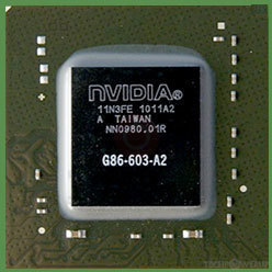
G86-603-A2

G86-613-A2
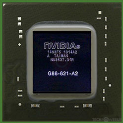
G86-621-A2

G86-631-A2

G86-635-A2

G86-827-A2
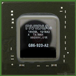
G86-920-A2

SIC66SIC66
Die Shot

TPC Diagram
NVIDIA's G86S GPU uses the Tesla architecture and is made using a 80 nm production process at TSMC. With a die size of 127 mm² and a transistor count of 210 million it is a small chip. G86S supports DirectX 11.1 (Feature Level 10_0). For GPU compute applications, OpenCL version 1.1 and CUDA 1.1 can be used. It features 16 shading units, 8 texture mapping units and 4 ROPs.
Further reading:
Tesla Architecture Whitepaper 
Graphics Processor
- Released
- Apr 17th, 2007
- GPU Name
- G86S
- Codename
- NV86
- Architecture
- Tesla
- Foundry
- TSMC
- Process Size
- 80 nm
- Transistors
- 210 million
- Density
- 1.7M / mm²
- Die Size
- 127 mm²
- Package
- BGA-533
Graphics Features
- DirectX
- 11.1 (10_0)
- OpenGL
- 3.3
- OpenCL
- 1.1
- Vulkan
- N/A
- CUDA
- 1.1
- Shader Model
- 4.0
- WDDM
- 1.2
- PureVideo HD
- VP2
- VDPAU
- Feature Set A
Render Config
- Shading Units
- 16
- TMUs
- 8
- ROPs
- 4
- SM Count
- 2
- SFUs
- 4
- TPCs
- 2
- Tex L1 Cache
- 16 KB per TPC
- L2 Cache
- 32 KB
- Max. TDP
- 50 W
All Tesla GPUs
NVIDIA GPU Architecture History
- 2023 Hopper
- 2022-2024 Ada Lovelace
- 2020-2024 Ampere
- 2018-2022 Turing
- 2017-2020 Volta
- 2016-2021 Pascal
- 2014-2019 Maxwell 2.0
- 2014-2017 Maxwell
- 2013-2015 Kepler 2.0
- 2012-2018 Kepler
- 2010-2016 Fermi 2.0
- 2010-2013 VLIW Vec4
- 2010-2016 Fermi
- 2007-2013 Tesla 2.0
- 2006-2010 Tesla
- 2003-2013 Curie
- 2003-2005 Rankine
- 2001-2003 Kelvin
- 1999-2005 Celsius
- 1998-2000 Fahrenheit
Graphics cards using the NVIDIA G86S GPU
| Name | Chip | Memory | Shaders | TMUs | ROPs | GPU Clock | Memory Clock |
|---|---|---|---|---|---|---|---|
| G86-213-A2 | 256 MB | 16 | 8 | 4 | 459 MHz | 400 MHz | |
| 128 MB | 8 | 8 | 4 | 459 MHz | 400 MHz | ||
| NB8M-GLM | 256 MB | 16 | 8 | 4 | 400 MHz | 400 MHz | |
| G86-827-A2 | 256 MB | 16 | 8 | 4 | 459 MHz | 400 MHz | |
| G86-613-A2 | 256 MB | 8 | 8 | 4 | 400 MHz | 700 MHz | |
| G86-621-A2 | 256 MB | 16 | 8 | 4 | 400 MHz | 594 MHz | |
| G86-740-A2 | 512 MB | 16 | 8 | 4 | 400 MHz | 600 MHz | |
| G86-635-A2 | 256 MB | 16 | 8 | 4 | 400 MHz | 400 MHz | |
| G86-603-A2 | 256 MB | 16 | 8 | 4 | 450 MHz | 602 MHz | |
| G86-630-A2 | 256 MB | 16 | 8 | 4 | 400 MHz | 400 MHz | |
| 128 MB | 16 | 8 | 4 | 459 MHz | 600 MHz | ||
| 128 MB | 16 | 8 | 4 | 459 MHz | 400 MHz |


G86S GPU Notes
| PureVideo HD: VP2 VDPAU: Feature Set A |
Apr 26th, 2024 03:50 EDT
change timezone
Latest GPU Drivers
New Forum Posts
- Which new games will you be buying? (320)
- Alphacool CORE 1 CPU block - bulging with danger of splitting? (21)
- TPU's Nostalgic Hardware Club (18467)
- Best SSD for system drive (82)
- What phone you use as your daily driver? And, a discussion of them. (1484)
- What's your latest tech purchase? (20342)
- AMD RX 7000 series GPU Owners' Club (1087)
- im new to throttelstop and i think i messed it up by copying others any hints would be very much aprreciated (3)
- Horizontal black lines popping up on my screen? (4)
- Black screen after muting (5)
Popular Reviews
- Fractal Design Terra Review
- Thermalright Phantom Spirit 120 EVO Review
- Corsair 2000D Airflow Review
- ASUS GeForce RTX 4090 STRIX OC Review
- NVIDIA GeForce RTX 4090 Founders Edition Review - Impressive Performance
- ASUS GeForce RTX 4090 Matrix Platinum Review - The RTX 4090 Ti
- MSI GeForce RTX 4090 Suprim X Review
- Gigabyte GeForce RTX 4090 Gaming OC Review
- MSI GeForce RTX 4090 Gaming X Trio Review
- MSI GeForce RTX 4090 Suprim Liquid X Review
Controversial News Posts
- Sony PlayStation 5 Pro Specifications Confirmed, Console Arrives Before Holidays (117)
- Windows 11 Now Officially Adware as Microsoft Embeds Ads in the Start Menu (117)
- NVIDIA Points Intel Raptor Lake CPU Users to Get Help from Intel Amid System Instability Issues (106)
- AMD "Strix Halo" Zen 5 Mobile Processor Pictured: Chiplet-based, Uses 256-bit LPDDR5X (101)
- US Government Wants Nuclear Plants to Offload AI Data Center Expansion (98)
- AMD's RDNA 4 GPUs Could Stick with 18 Gbps GDDR6 Memory (88)
- Developers of Outpost Infinity Siege Recommend Underclocking i9-13900K and i9-14900K for Stability on Machines with RTX 4090 (85)
- Windows 10 Security Updates to Cost $61 After 2025, $427 by 2028 (84)