Report an Error
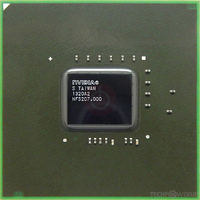


NVIDIA GF117B

GF117B

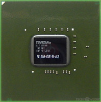
N13M-GE-B-A2

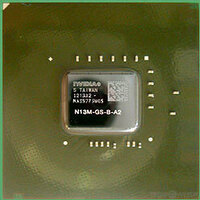
N13M-GS-B-A2

N14M-GL-B-A2

N15V-GM-B-A2
NVIDIA's GF117B GPU uses the Fermi 2.0 architecture and is made using a 28 nm production process at TSMC. With a die size of 116 mm² and a transistor count of 585 million it is a small chip. GF117B supports DirectX 12 (Feature Level 11_0). For GPU compute applications, OpenCL version 1.1 and CUDA 2.1 can be used. It features 96 shading units, 16 texture mapping units and 8 ROPs.
Further reading:
Fermi Compute Architecture 
Graphics Processor
- Released
- Dec 1st, 2011
- GPU Name
- GF117B
- Codename
- NVD7
- Architecture
- Fermi 2.0
- Foundry
- TSMC
- Process Size
- 28 nm
- Transistors
- 585 million
- Density
- 5.0M / mm²
- Die Size
- 116 mm²
- Package
- BGA-908
Graphics Features
- DirectX
- 12 (11_0)
- OpenGL
- 4.6
- OpenCL
- 1.1
- Vulkan
- N/A
- CUDA
- 2.1
- Shader Model
- 5.1
- WDDM
- 2.3
- PureVideo HD
- VP5
- VDPAU
- Feature Set D
Render Config
- Shading Units
- 96
- TMUs
- 16
- ROPs
- 8
- SM Count
- 4
- SFUs
- 16
- GPCs
- 1
- L1 Cache
- 64 KB per SM
- L2 Cache
- 128 KB
- Max. TDP
- 15 W
All Fermi 2.0 GPUs
NVIDIA GPU Architecture History
- 2024 Blackwell
- 2023 Hopper
- 2022-2024 Ada Lovelace
- 2020-2024 Ampere
- 2018-2022 Turing
- 2017-2020 Volta
- 2016-2021 Pascal
- 2014-2019 Maxwell 2.0
- 2014-2017 Maxwell
- 2013-2015 Kepler 2.0
- 2012-2018 Kepler
- 2010-2016 Fermi 2.0
- 2010-2013 VLIW Vec4
- 2010-2016 Fermi
- 2007-2013 Tesla 2.0
- 2006-2010 Tesla
- 2003-2013 Curie
- 2003-2005 Rankine
- 2001-2003 Kelvin
- 1999-2005 Celsius
- 1998-2000 Fahrenheit
Graphics cards using the NVIDIA GF117B GPU
| Name | Chip | Memory | Shaders | TMUs | ROPs | GPU Clock | Memory Clock |
|---|---|---|---|---|---|---|---|
| N13M-GS-B-A2 | 2 GB | 96 | 16 | 4 | 625 MHz | 800 MHz | |
| N14M-GL-B-A2 | 1024 MB | 48 | 8 | 8 | 625 MHz | 900 MHz | |
| N15V-GM-B-A2 | 1024 MB | 96 | 16 | 8 | 625 MHz | 900 MHz |


GF117B GPU Notes
| PureVideo HD: VP5 VDPAU: Feature Set D |
May 1st, 2024 13:02 EDT
change timezone
Latest GPU Drivers
New Forum Posts
- TPU's Rosetta Milestones and Daily Pie Thread (1865)
- Alphacool CORE 1 CPU block - bulging with danger of splitting? (56)
- Recommendation for Android gaming tablet? (2)
- MSI Stealth GS65 9SF settings after repaste (1)
- Old high quality PSU, or semi-old mid-quality PSU? (21)
- Is this Sapphire PULSE RX 5600 XT legit or fake? (23)
- Throttlestop stopped working (VBS is disabled) (1)
- Story saver apps to Instagram (1)
- PC Game Retro Reviews (28)
- DTS DCH Driver for Realtek HDA [DTS:X APO4 + DTS Interactive] (1911)
Popular Reviews
- Ugreen NASync DXP4800 Plus Review
- Team Group T-Force Vulcan ECO DDR5-6000 32 GB CL38 Review
- HYTE THICC Q60 240 mm AIO Review
- Upcoming Hardware Launches 2023 (Updated Feb 2024)
- MOONDROP x Crinacle DUSK In-Ear Monitors Review - The Last 5%
- Montech Sky Two GX Review
- Thermalright Phantom Spirit 120 EVO Review
- AMD Ryzen 7 7800X3D Review - The Best Gaming CPU
- ASUS Radeon RX 7900 GRE TUF OC Review
- FiiO K19 Desktop DAC/Headphone Amplifier Review
Controversial News Posts
- Intel Statement on Stability Issues: "Motherboard Makers to Blame" (210)
- Windows 11 Now Officially Adware as Microsoft Embeds Ads in the Start Menu (157)
- Sony PlayStation 5 Pro Specifications Confirmed, Console Arrives Before Holidays (117)
- AMD's RDNA 4 GPUs Could Stick with 18 Gbps GDDR6 Memory (109)
- NVIDIA Points Intel Raptor Lake CPU Users to Get Help from Intel Amid System Instability Issues (106)
- AMD "Strix Halo" Zen 5 Mobile Processor Pictured: Chiplet-based, Uses 256-bit LPDDR5X (103)
- TechPowerUp Hiring: Reviewers Wanted for Motherboards, Laptops, Gaming Handhelds and Prebuilt Desktops (90)
- Superior Stability by GIGABYTE BETA BIOS with Intel Baseline on Z790/B760 Motherboards (86)