Report an Error


NVIDIA Quadro FX 570
- Graphics Processor
- G84
- Cores
- 16
- TMUs
- 8
- ROPs
- 8
- Memory Size
- 256 MB
- Memory Type
- DDR2
- Bus Width
- 128 bit

GPU
I/O
Bottom

Back
Recommended Gaming Resolutions:
- 640x480
- 1280x720
- 1366x768
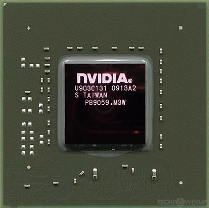
The Quadro FX 570 was a performance-segment professional graphics card by NVIDIA, launched on September 12th, 2007. Built on the 80 nm process, and based on the G84 graphics processor, the card supports DirectX 11.1. Even though it supports DirectX 11, the feature level is only 10_0, which can be problematic with many DirectX 11 & DirectX 12 titles. The G84 graphics processor is an average sized chip with a die area of 169 mm² and 289 million transistors. Unlike the fully unlocked GeForce 8600 GT Mac Edition, which uses the same GPU but has all 32 shaders enabled, NVIDIA has disabled some shading units on the Quadro FX 570 to reach the product's target shader count. It features 16 shading units, 8 texture mapping units, and 8 ROPs. NVIDIA has paired 256 MB DDR2 memory with the Quadro FX 570, which are connected using a 128-bit memory interface. The GPU is operating at a frequency of 460 MHz, memory is running at 400 MHz.
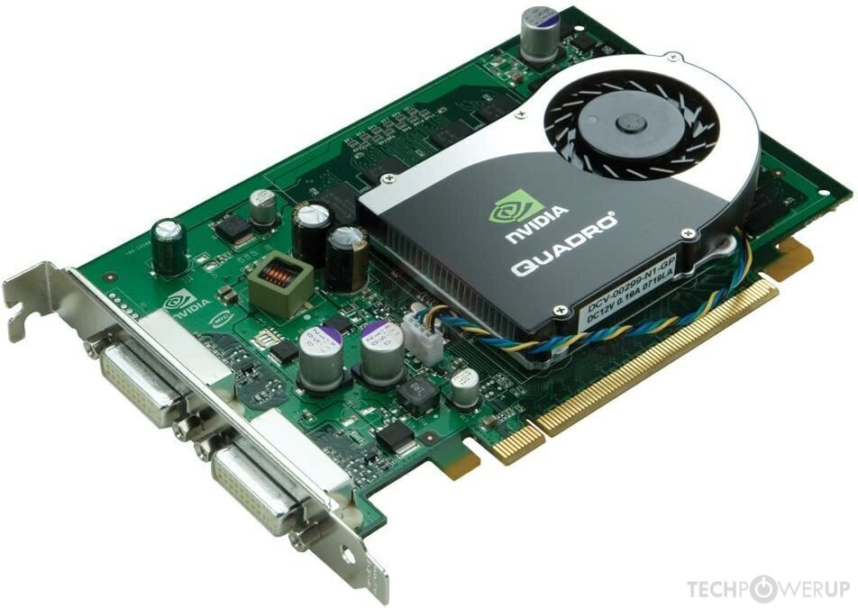
Being a single-slot card, the NVIDIA Quadro FX 570 does not require any additional power connector, its power draw is rated at 38 W maximum. Display outputs include: 2x DVI. Quadro FX 570 is connected to the rest of the system using a PCI-Express 1.0 x16 interface. The card measures 198 mm in length, 111 mm in width, and features a single-slot cooling solution. Its price at launch was 199 US Dollars.
Being a single-slot card, the NVIDIA Quadro FX 570 does not require any additional power connector, its power draw is rated at 38 W maximum. Display outputs include: 2x DVI. Quadro FX 570 is connected to the rest of the system using a PCI-Express 1.0 x16 interface. The card measures 198 mm in length, 111 mm in width, and features a single-slot cooling solution. Its price at launch was 199 US Dollars.
Graphics Processor
Graphics Card
- Release Date
- Sep 12th, 2007
- Generation
-
Quadro FX Tesla
(x700)
- Predecessor
- Quadro FX Curie
- Successor
- Quadro Fermi
- Production
- End-of-life
- Launch Price
- 199 USD
- Bus Interface
- PCIe 1.0 x16
- Reviews
- 26 in our database
Relative Performance
Based on TPU review data: "Performance Summary" at 1920x1080, 4K for 2080 Ti and faster.
Performance estimated based on architecture, shader count and clocks.
Clock Speeds
- GPU Clock
- 460 MHz
- Shader Clock
- 920 MHz
- Memory Clock
-
400 MHz
800 Mbps effective
Memory
- Memory Size
- 256 MB
- Memory Type
- DDR2
- Memory Bus
- 128 bit
- Bandwidth
- 12.80 GB/s
Render Config
- Shading Units
- 16
- TMUs
- 8
- ROPs
- 8
- SM Count
- 2
- L2 Cache
- 32 KB
Theoretical Performance
- Pixel Rate
- 3.680 GPixel/s
- Texture Rate
- 3.680 GTexel/s
- FP32 (float)
- 29.44 GFLOPS
Board Design
- Slot Width
- Single-slot
- Length
- 198 mm
7.8 inches
- Width
- 111 mm
4.4 inches
- TDP
- 38 W
- Suggested PSU
- 200 W
- Outputs
- 2x DVI
- Power Connectors
- None
- Board Number
- P588 SKU 500
Graphics Features
- DirectX
- 11.1 (10_0)
- OpenGL
- 3.3
- OpenCL
- 1.1
- Vulkan
- N/A
- CUDA
- 1.1
- Shader Model
- 4.0
G84 GPU Notes
| PureVideo HD: VP2 VDPAU: Feature Set A |
Apr 26th, 2024 16:58 EDT
change timezone
Latest GPU Drivers
New Forum Posts
- Alphacool CORE 1 CPU block - bulging with danger of splitting? (30)
- Dell Workstation Owners Club (3061)
- Xeon Owners Club (8700)
- Secure boot already open help (10)
- hacked (77)
- Best SSD for system drive (92)
- looking to build a new system and im considering asrock brand but i have some doubts/concerns. (4)
- Meta Horizon OS (22)
- Windows 11 General Discussion (5024)
- problems flashing default bios to dual-bios rx 480 card (6)
Popular Reviews
- HYTE THICC Q60 240 mm AIO Review
- MOONDROP x Crinacle DUSK In-Ear Monitors Review - The Last 5%
- Upcoming Hardware Launches 2023 (Updated Feb 2024)
- Alienware Pro Wireless Gaming Keyboard Review
- Thermalright Phantom Spirit 120 EVO Review
- FiiO K19 Desktop DAC/Headphone Amplifier Review
- ASUS Radeon RX 7900 GRE TUF OC Review
- AMD Ryzen 7 7800X3D Review - The Best Gaming CPU
- RTX 4090 & 53 Games: Ryzen 7 5800X vs Ryzen 7 5800X3D Review
- Sapphire Radeon RX 7900 GRE Pulse Review
Controversial News Posts
- Windows 11 Now Officially Adware as Microsoft Embeds Ads in the Start Menu (135)
- Sony PlayStation 5 Pro Specifications Confirmed, Console Arrives Before Holidays (117)
- NVIDIA Points Intel Raptor Lake CPU Users to Get Help from Intel Amid System Instability Issues (106)
- AMD "Strix Halo" Zen 5 Mobile Processor Pictured: Chiplet-based, Uses 256-bit LPDDR5X (103)
- US Government Wants Nuclear Plants to Offload AI Data Center Expansion (98)
- AMD's RDNA 4 GPUs Could Stick with 18 Gbps GDDR6 Memory (95)
- Developers of Outpost Infinity Siege Recommend Underclocking i9-13900K and i9-14900K for Stability on Machines with RTX 4090 (85)
- Windows 10 Security Updates to Cost $61 After 2025, $427 by 2028 (84)