Report an Error


AMD Radeon VII
- Graphics Processor
- Vega 20
- Cores
- 3840
- TMUs
- 240
- ROPs
- 64
- Memory Size
- 16 GB
- Memory Type
- HBM2
- Bus Width
- 4096 bit
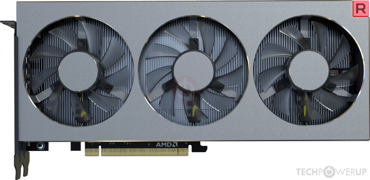

GPU
I/O
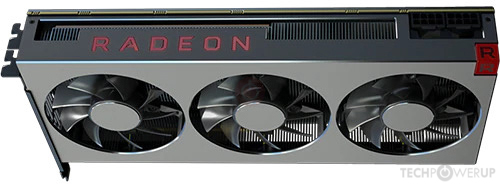
Top

Bottom

Back

PCB Front
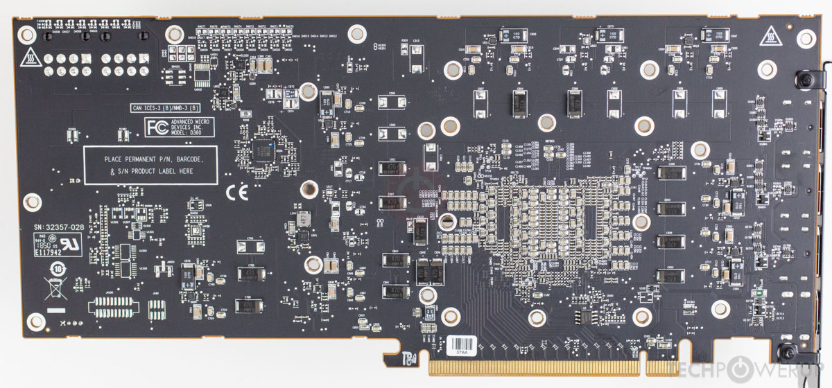
PCB Back
Recommended Gaming Resolutions:
- 1920x1080
- 2560x1440
- 3840x2160
The Radeon VII is an enthusiast-class graphics card by AMD, launched on February 7th, 2019. Built on the 7 nm process, and based on the Vega 20 graphics processor, in its Vega 20 XT variant, the card supports DirectX 12. This ensures that all modern games will run on Radeon VII. The Vega 20 graphics processor is a large chip with a die area of 331 mm² and 13,230 million transistors. It features 3840 shading units, 240 texture mapping units, and 64 ROPs. AMD has paired 16 GB HBM2 memory with the Radeon VII, which are connected using a 4096-bit memory interface. The GPU is operating at a frequency of 1400 MHz, which can be boosted up to 1750 MHz, memory is running at 1000 MHz.
Being a dual-slot card, the AMD Radeon VII draws power from 2x 8-pin power connectors, with power draw rated at 295 W maximum. Display outputs include: 1x HDMI 2.0b, 3x DisplayPort 1.4a. Radeon VII is connected to the rest of the system using a PCI-Express 3.0 x16 interface. The card's dimensions are 280 mm x 125 mm x 40 mm, and it features a dual-slot cooling solution. Its price at launch was 699 US Dollars.
Being a dual-slot card, the AMD Radeon VII draws power from 2x 8-pin power connectors, with power draw rated at 295 W maximum. Display outputs include: 1x HDMI 2.0b, 3x DisplayPort 1.4a. Radeon VII is connected to the rest of the system using a PCI-Express 3.0 x16 interface. The card's dimensions are 280 mm x 125 mm x 40 mm, and it features a dual-slot cooling solution. Its price at launch was 699 US Dollars.
Graphics Processor
Graphics Card
Relative Performance
Based on TPU review data: "Performance Summary" at 1920x1080, 4K for 2080 Ti and faster.
Clock Speeds
- Base Clock
- 1400 MHz
- Boost Clock
- 1750 MHz
- Peak Clock
- 1802 MHz
- Memory Clock
-
1000 MHz
2 Gbps effective
Memory
- Memory Size
- 16 GB
- Memory Type
- HBM2
- Memory Bus
- 4096 bit
- Bandwidth
- 1.02 TB/s
Render Config
- Shading Units
- 3840
- TMUs
- 240
- ROPs
- 64
- Compute Units
- 60
- L1 Cache
- 16 KB (per CU)
- L2 Cache
- 4 MB
Theoretical Performance
- Pixel Rate
- 112.0 GPixel/s
- Texture Rate
- 420.0 GTexel/s
- FP16 (half)
- 26.88 TFLOPS (2:1)
- FP32 (float)
- 13.44 TFLOPS
- FP64 (double)
- 3.360 TFLOPS (1:4)
Board Design
- Slot Width
- Dual-slot
- Length
- 280 mm
11 inches
- Width
- 125 mm
4.9 inches
- Height
- 40 mm
1.6 inches
- TDP
- 295 W
- Suggested PSU
- 600 W
- Outputs
- 1x HDMI 2.0b
3x DisplayPort 1.4a
- Power Connectors
- 2x 8-pin
- Board Number
- 109-D36037-00_04
- BIOS Number
- 113-D3600200-105
Graphics Features
- DirectX
- 12 (12_1)
- OpenGL
- 4.6
- OpenCL
- 2.1
- Vulkan
- 1.3
- Shader Model
- 6.7
Vega 20 GPU Notes
| Generation: Vega II Codename: Moonshot Old Codename: Aruba Graphics/Compute: 9.4.0 Shader ISA: GFX9 (gfx906 / gfx907) Display Core Engine: 12.1 Unified Video Decoder: 7.2 Video Compression Engine: 4.1 System DMA: 4.2.0 Platform Security Processor: 11.0.2 CLRX: GCN 1.4.1 |
Retail boards based on this design (13)
| Name | GPU Clock | Boost Clock | Memory Clock | Other Changes |
|---|---|---|---|---|
| 1400 MHz | 1750 MHz | 1000 MHz | ||
| 1400 MHz | 1750 MHz | 1000 MHz | ||
| 1400 MHz | 1750 MHz | 1000 MHz | ||
| 1400 MHz | 1750 MHz | 1000 MHz | ||
| 1400 MHz | 1750 MHz | 1000 MHz | ||
| 1400 MHz | 1750 MHz | 1000 MHz | ||
| 1400 MHz | 1750 MHz | 1000 MHz | ||
| 1400 MHz | 1750 MHz | 1000 MHz | ||
| 1400 MHz | 1750 MHz | 1000 MHz | ||
| 1400 MHz | 1750 MHz | 1000 MHz | ||
| 1400 MHz | 1750 MHz | 1000 MHz | ||
| 1400 MHz | 1750 MHz | 1000 MHz | ||
| 1400 MHz | 1750 MHz | 1000 MHz |


Apr 27th, 2024 05:13 EDT
change timezone
Latest GPU Drivers
New Forum Posts
- hacked (79)
- Ryzen Owners Zen Garden (7247)
- Post your Speedtest.net Speeds! (2256)
- Should I install Windows 10 or 11 for my new device (5)
- TechPowerUp Screenshot Thread (MASSIVE 56K WARNING) (4214)
- wireless mic for pc (1)
- My mouse randomly stops working (2)
- Horizontal black lines popping up on my screen? (14)
- MSI Stealth GS65 9SF settings after repaste (0)
- Which terminal emulator do you use the most? (10)
Popular Reviews
- Ugreen NASync DXP4800 Plus Review
- HYTE THICC Q60 240 mm AIO Review
- MOONDROP x Crinacle DUSK In-Ear Monitors Review - The Last 5%
- Upcoming Hardware Launches 2023 (Updated Feb 2024)
- Thermalright Phantom Spirit 120 EVO Review
- FiiO K19 Desktop DAC/Headphone Amplifier Review
- Quick Look: MOONDROP CHU 2 Budget In-Ear Monitors
- AMD Ryzen 7 7800X3D Review - The Best Gaming CPU
- Alienware Pro Wireless Gaming Keyboard Review
- ASUS Radeon RX 7900 GRE TUF OC Review
Controversial News Posts
- Windows 11 Now Officially Adware as Microsoft Embeds Ads in the Start Menu (137)
- Sony PlayStation 5 Pro Specifications Confirmed, Console Arrives Before Holidays (117)
- NVIDIA Points Intel Raptor Lake CPU Users to Get Help from Intel Amid System Instability Issues (106)
- AMD "Strix Halo" Zen 5 Mobile Processor Pictured: Chiplet-based, Uses 256-bit LPDDR5X (103)
- US Government Wants Nuclear Plants to Offload AI Data Center Expansion (98)
- AMD's RDNA 4 GPUs Could Stick with 18 Gbps GDDR6 Memory (95)
- Developers of Outpost Infinity Siege Recommend Underclocking i9-13900K and i9-14900K for Stability on Machines with RTX 4090 (85)
- Windows 10 Security Updates to Cost $61 After 2025, $427 by 2028 (84)