Report an Error


NVIDIA RTX 4500 Ada Generation
- Graphics Processor
- AD103
- Cores
- 7680
- TMUs
- 240
- ROPs
- 80
- Memory Size
- 24 GB
- Memory Type
- GDDR6
- Bus Width
- 192 bit


GPU
I/O

Back
Recommended Gaming Resolutions:
- 1920x1080
- 2560x1440
- 3840x2160
The RTX 4500 Ada Generation is a professional graphics card by NVIDIA, launched on August 9th, 2023. Built on the 5 nm process, and based on the AD103 graphics processor, the card supports DirectX 12 Ultimate. The AD103 graphics processor is a large chip with a die area of 379 mm² and 45,900 million transistors. Unlike the fully unlocked GeForce RTX 4080 SUPER, which uses the same GPU but has all 10240 shaders enabled, NVIDIA has disabled some shading units on the RTX 4500 Ada Generation to reach the product's target shader count. It features 7680 shading units, 240 texture mapping units, and 80 ROPs. Also included are 240 tensor cores which help improve the speed of machine learning applications. The card also has 60 raytracing acceleration cores. NVIDIA has paired 24 GB GDDR6 memory with the RTX 4500 Ada Generation, which are connected using a 192-bit memory interface. The GPU is operating at a frequency of 2070 MHz, which can be boosted up to 2580 MHz, memory is running at 2250 MHz (18 Gbps effective).
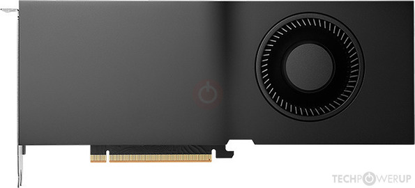
Being a dual-slot card, the NVIDIA RTX 4500 Ada Generation does not require any additional power connector, its power draw is rated at 210 W maximum. Display outputs include: 4x DisplayPort 1.4a. RTX 4500 Ada Generation is connected to the rest of the system using a PCI-Express 4.0 x16 interface. The card measures 245 mm in length, 112 mm in width, and features a dual-slot cooling solution.
Being a dual-slot card, the NVIDIA RTX 4500 Ada Generation does not require any additional power connector, its power draw is rated at 210 W maximum. Display outputs include: 4x DisplayPort 1.4a. RTX 4500 Ada Generation is connected to the rest of the system using a PCI-Express 4.0 x16 interface. The card measures 245 mm in length, 112 mm in width, and features a dual-slot cooling solution.
Graphics Processor
- GPU Name
- AD103
- Architecture
- Ada Lovelace
- Foundry
- TSMC
- Process Size
- 5 nm
- Transistors
- 45,900 million
- Density
- 121.1M / mm²
- Die Size
- 379 mm²
Graphics Card
- Release Date
- Aug 9th, 2023
- Generation
-
Quadro Ada
(x000A)
- Predecessor
- Quadro Ampere
- Production
- Active
- Bus Interface
- PCIe 4.0 x16
Relative Performance
Based on TPU review data: "Performance Summary" at 1920x1080, 4K for 2080 Ti and faster.
Performance estimated based on architecture, shader count and clocks.
Clock Speeds
- Base Clock
- 2070 MHz
- Boost Clock
- 2580 MHz
- Memory Clock
-
2250 MHz
18 Gbps effective
Memory
- Memory Size
- 24 GB
- Memory Type
- GDDR6
- Memory Bus
- 192 bit
- Bandwidth
- 432.0 GB/s
Render Config
- Shading Units
- 7680
- TMUs
- 240
- ROPs
- 80
- SM Count
- 60
- Tensor Cores
- 240
- RT Cores
- 60
- L1 Cache
- 128 KB (per SM)
- L2 Cache
- 48 MB
Theoretical Performance
- Pixel Rate
- 206.4 GPixel/s
- Texture Rate
- 619.2 GTexel/s
- FP16 (half)
- 39.63 TFLOPS (1:1)
- FP32 (float)
- 39.63 TFLOPS
- FP64 (double)
- 619.2 GFLOPS (1:64)
Board Design
- Slot Width
- Dual-slot
- Length
- 245 mm
9.6 inches
- Width
- 112 mm
4.4 inches
- TDP
- 210 W
- Suggested PSU
- 550 W
- Outputs
- 4x DisplayPort 1.4a
- Power Connectors
- None
Graphics Features
- DirectX
- 12 Ultimate (12_2)
- OpenGL
- 4.6
- OpenCL
- 3.0
- Vulkan
- 1.3
- CUDA
- 8.9
- Shader Model
- 6.7
Card Notes
| 2 NVENC Engines 2 NVDEC Engines |
AD103 GPU Notes
| Ray Tracing Cores: 3rd Gen Tensor Cores: 4th Gen NVENC: 8th Gen NVDEC: 5th Gen PureVideo HD: VP12 VDPAU: Feature Set L |
Apr 28th, 2024 04:27 EDT
change timezone
Latest GPU Drivers
New Forum Posts
- Arctic P14 MAX fans (3)
- Starfield discussion thread (1634)
- Games that require more 24 VRAM... (75)
- Shadow Of The Tomb Raider - CPU Performance and general game benchmark discussions (525)
- Looking for recommendations to upgrade the GPU (18)
- Best SSD for system drive (110)
- Which PSU to take? (6)
- HyperX mechanical keyboards (2)
- AMD RX 7000 series GPU Owners' Club (1089)
- Which air cooler for a ryzen 9 5900x (173)
Popular Reviews
- Ugreen NASync DXP4800 Plus Review
- HYTE THICC Q60 240 mm AIO Review
- MOONDROP x Crinacle DUSK In-Ear Monitors Review - The Last 5%
- Upcoming Hardware Launches 2023 (Updated Feb 2024)
- Thermalright Phantom Spirit 120 EVO Review
- AMD Ryzen 7 7800X3D Review - The Best Gaming CPU
- FiiO K19 Desktop DAC/Headphone Amplifier Review
- Intel Core i9-14900KS Review - The Last of its Kind
- ASUS Radeon RX 7900 GRE TUF OC Review
- Alienware Pro Wireless Gaming Keyboard Review
Controversial News Posts
- Windows 11 Now Officially Adware as Microsoft Embeds Ads in the Start Menu (139)
- Sony PlayStation 5 Pro Specifications Confirmed, Console Arrives Before Holidays (117)
- NVIDIA Points Intel Raptor Lake CPU Users to Get Help from Intel Amid System Instability Issues (106)
- AMD "Strix Halo" Zen 5 Mobile Processor Pictured: Chiplet-based, Uses 256-bit LPDDR5X (103)
- US Government Wants Nuclear Plants to Offload AI Data Center Expansion (98)
- AMD's RDNA 4 GPUs Could Stick with 18 Gbps GDDR6 Memory (95)
- Developers of Outpost Infinity Siege Recommend Underclocking i9-13900K and i9-14900K for Stability on Machines with RTX 4090 (85)
- Windows 10 Security Updates to Cost $61 After 2025, $427 by 2028 (84)