Report an Error


NVIDIA RTX 6000 Ada Generation
- Graphics Processor
- AD102
- Cores
- 18176
- TMUs
- 568
- ROPs
- 192
- Memory Size
- 48 GB
- Memory Type
- GDDR6
- Bus Width
- 384 bit


GPU
I/O

Top
Recommended Gaming Resolutions:
- 1920x1080
- 2560x1440
- 3840x2160
The RTX 6000 Ada Generation is an enthusiast-class professional graphics card by NVIDIA, launched on December 3rd, 2022. Built on the 5 nm process, and based on the AD102 graphics processor, in its AD102 variant, the card supports DirectX 12 Ultimate. The AD102 graphics processor is a large chip with a die area of 609 mm² and 76,300 million transistors. Unlike the fully unlocked TITAN Ada, which uses the same GPU but has all 18432 shaders enabled, NVIDIA has disabled some shading units on the RTX 6000 Ada Generation to reach the product's target shader count. It features 18176 shading units, 568 texture mapping units, and 192 ROPs. Also included are 568 tensor cores which help improve the speed of machine learning applications. The card also has 142 raytracing acceleration cores. NVIDIA has paired 48 GB GDDR6 memory with the RTX 6000 Ada Generation, which are connected using a 384-bit memory interface. The GPU is operating at a frequency of 915 MHz, which can be boosted up to 2505 MHz, memory is running at 2500 MHz (20 Gbps effective).
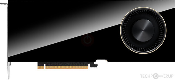
Being a dual-slot card, the NVIDIA RTX 6000 Ada Generation draws power from 1x 16-pin power connector, with power draw rated at 300 W maximum. Display outputs include: 4x DisplayPort 1.4a. RTX 6000 Ada Generation is connected to the rest of the system using a PCI-Express 4.0 x16 interface. The card measures 267 mm in length, 112 mm in width, and features a dual-slot cooling solution. Its price at launch was 6799 US Dollars.
Being a dual-slot card, the NVIDIA RTX 6000 Ada Generation draws power from 1x 16-pin power connector, with power draw rated at 300 W maximum. Display outputs include: 4x DisplayPort 1.4a. RTX 6000 Ada Generation is connected to the rest of the system using a PCI-Express 4.0 x16 interface. The card measures 267 mm in length, 112 mm in width, and features a dual-slot cooling solution. Its price at launch was 6799 US Dollars.
Graphics Processor
- GPU Name
- AD102
- GPU Variant
- AD102
- Architecture
- Ada Lovelace
- Foundry
- TSMC
- Process Size
- 5 nm
- Transistors
- 76,300 million
- Density
- 125.3M / mm²
- Die Size
- 609 mm²
Graphics Card
- Release Date
- Dec 3rd, 2022
- Availability
- Jan 20th, 2023
- Generation
-
Quadro Ada
(x000A)
- Predecessor
- Quadro Ampere
- Production
- Active
- Launch Price
- 6,799 USD
- Bus Interface
- PCIe 4.0 x16
Relative Performance
Based on TPU review data: "Performance Summary" at 1920x1080, 4K for 2080 Ti and faster.
Performance estimated based on architecture, shader count and clocks.
Clock Speeds
- Base Clock
- 915 MHz
- Boost Clock
- 2505 MHz
- Memory Clock
-
2500 MHz
20 Gbps effective
Memory
- Memory Size
- 48 GB
- Memory Type
- GDDR6
- Memory Bus
- 384 bit
- Bandwidth
- 960.0 GB/s
Render Config
- Shading Units
- 18176
- TMUs
- 568
- ROPs
- 192
- SM Count
- 142
- Tensor Cores
- 568
- RT Cores
- 142
- L1 Cache
- 128 KB (per SM)
- L2 Cache
- 96 MB
Theoretical Performance
- Pixel Rate
- 481.0 GPixel/s
- Texture Rate
- 1,423 GTexel/s
- FP16 (half)
- 91.06 TFLOPS (1:1)
- FP32 (float)
- 91.06 TFLOPS
- FP64 (double)
- 1,423 GFLOPS (1:64)
Board Design
- Slot Width
- Dual-slot
- Length
- 267 mm
10.5 inches
- Width
- 112 mm
4.4 inches
- TDP
- 300 W
- Suggested PSU
- 700 W
- Outputs
- 4x DisplayPort 1.4a
- Power Connectors
- 1x 16-pin
Graphics Features
- DirectX
- 12 Ultimate (12_2)
- OpenGL
- 4.6
- OpenCL
- 3.0
- Vulkan
- 1.3
- CUDA
- 8.9
- Shader Model
- 6.7
Card Notes
| 3 NVENC Engines 3 NVDEC Engines |
AD102 GPU Notes
| Ray Tracing Cores: 3rd Gen Tensor Cores: 4th Gen NVENC: 8th Gen NVDEC: 5th Gen PureVideo HD: VP12 VDPAU: Feature Set L |
Retail boards based on this design (1)
| Name | GPU Clock | Boost Clock | Memory Clock | Other Changes |
|---|---|---|---|---|
| 915 MHz | 2505 MHz | 2500 MHz |

Apr 26th, 2024 11:40 EDT
change timezone
Latest GPU Drivers
New Forum Posts
- im new to throttelstop and i think i messed it up by copying others any hints would be very much aprreciated (4)
- The TPU UK Clubhouse (24787)
- Cs2 Freezing in Rx 580 (5)
- Ghost of Tsushima PC Port !!!! (15)
- The Official Linux/Unix Desktop Screenshots Megathread (699)
- Red Dead Redemption using emu (4)
- Meta Horizon OS (21)
- Old high quality PSU, or semi-old mid-quality PSU? (3)
- Secure boot already open help (8)
- What are you playing? (20540)
Popular Reviews
- HYTE THICC Q60 240 mm AIO Review
- MOONDROP x Crinacle DUSK In-Ear Monitors Review - The Last 5%
- Alienware Pro Wireless Gaming Keyboard Review
- Upcoming Hardware Launches 2023 (Updated Feb 2024)
- Thermalright Phantom Spirit 120 EVO Review
- ASUS Radeon RX 7900 GRE TUF OC Review
- FiiO K19 Desktop DAC/Headphone Amplifier Review
- RTX 4090 & 53 Games: Ryzen 7 5800X vs Ryzen 7 5800X3D Review
- NVIDIA RTX 4090: 450 W vs 600 W 12VHPWR - Is there any notable performance difference?
- Sapphire Radeon RX 7900 GRE Pulse Review
Controversial News Posts
- Windows 11 Now Officially Adware as Microsoft Embeds Ads in the Start Menu (125)
- Sony PlayStation 5 Pro Specifications Confirmed, Console Arrives Before Holidays (117)
- NVIDIA Points Intel Raptor Lake CPU Users to Get Help from Intel Amid System Instability Issues (106)
- AMD "Strix Halo" Zen 5 Mobile Processor Pictured: Chiplet-based, Uses 256-bit LPDDR5X (101)
- US Government Wants Nuclear Plants to Offload AI Data Center Expansion (98)
- AMD's RDNA 4 GPUs Could Stick with 18 Gbps GDDR6 Memory (92)
- Developers of Outpost Infinity Siege Recommend Underclocking i9-13900K and i9-14900K for Stability on Machines with RTX 4090 (85)
- Windows 10 Security Updates to Cost $61 After 2025, $427 by 2028 (84)