Report an Error


ATI Radeon HD 4810
- Graphics Processor
- RV770
- Cores
- 640
- TMUs
- 32
- ROPs
- 8
- Memory Size
- 512 MB
- Memory Type
- GDDR5
- Bus Width
- 128 bit

GPU
Recommended Gaming Resolutions:
- 1366x768
- 1600x900
- 1920x1080
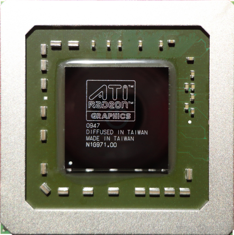
The Radeon HD 4810 was a graphics card by ATI, launched on May 28th, 2009. Built on the 55 nm process, and based on the RV770 graphics processor, in its RV770 CE variant, the card supports DirectX 10.1. Since Radeon HD 4810 does not support DirectX 11 or DirectX 12, it might not be able to run all the latest games. The RV770 graphics processor is an average sized chip with a die area of 256 mm² and 956 million transistors. Unlike the fully unlocked Radeon HD 4870, which uses the same GPU but has all 800 shaders enabled, ATI has disabled some shading units on the Radeon HD 4810 to reach the product's target shader count. It features 640 shading units, 32 texture mapping units, and 8 ROPs. ATI has paired 512 MB GDDR5 memory with the Radeon HD 4810, which are connected using a 128-bit memory interface. The GPU is operating at a frequency of 625 MHz, memory is running at 900 MHz (3.6 Gbps effective).
Being a single-slot card, the ATI Radeon HD 4810 draws power from 1x 6-pin power connector, with power draw rated at 95 W maximum. Display outputs include: 2x DVI, 1x S-Video. Radeon HD 4810 is connected to the rest of the system using a PCI-Express 2.0 x16 interface. The card measures 246 mm in length, and features a single-slot cooling solution.
Being a single-slot card, the ATI Radeon HD 4810 draws power from 1x 6-pin power connector, with power draw rated at 95 W maximum. Display outputs include: 2x DVI, 1x S-Video. Radeon HD 4810 is connected to the rest of the system using a PCI-Express 2.0 x16 interface. The card measures 246 mm in length, and features a single-slot cooling solution.
Graphics Processor
Graphics Card
- Release Date
- May 28th, 2009
- Generation
-
Radeon R700
(HD 4800)
- Predecessor
- Radeon R600
- Successor
- Evergreen
- Production
- End-of-life
- Bus Interface
- PCIe 2.0 x16
Relative Performance
Based on TPU review data: "Performance Summary" at 1920x1080, 4K for 2080 Ti and faster.
Performance estimated based on architecture, shader count and clocks.
Clock Speeds
- GPU Clock
- 625 MHz
- Memory Clock
-
900 MHz
3.6 Gbps effective
Memory
- Memory Size
- 512 MB
- Memory Type
- GDDR5
- Memory Bus
- 128 bit
- Bandwidth
- 57.60 GB/s
Render Config
- Shading Units
- 640
- TMUs
- 32
- ROPs
- 8
- Compute Units
- 8
- L1 Cache
- 16 KB (per CU)
- L2 Cache
- 128 KB
Theoretical Performance
- Pixel Rate
- 5.000 GPixel/s
- Texture Rate
- 20.00 GTexel/s
- FP32 (float)
- 800.0 GFLOPS
- FP64 (double)
- 160.0 GFLOPS (1:5)
Board Design
- Slot Width
- Single-slot
- Length
- 246 mm
9.7 inches
- TDP
- 95 W
- Suggested PSU
- 250 W
- Outputs
- 2x DVI
1x S-Video
- Power Connectors
- 1x 6-pin
- Board Number
- B507
Graphics Features
- DirectX
- 10.1 (10_1)
- OpenGL
- 3.3
- OpenCL
- 1.1
- Vulkan
- N/A
- Shader Model
- 4.1
RV770 GPU Notes
| Mobile Variant: M98 Codename: Wekiva Graphics/Compute: GFX3 Display Core Engine: 3.1 Unified Video Decoder: 2.0 |
Retail boards based on this design (2)
| Name | GPU Clock | Memory Clock | Other Changes |
|---|---|---|---|
| 625 MHz | 900 MHz | 1x DVI 1x HDMI 1x VGA | |
| 750 MHz | 900 MHz | 1x DVI 1x HDMI 1x VGA |


May 18th, 2024 03:29 EDT
change timezone
Latest GPU Drivers
New Forum Posts
- is there anyway to verify my motherboard actually has a gen5 gpu slot without a gen5 card? (8)
- Homeworld 3 [Official Thread] (47)
- AMD Ryzen 7 7800X3D $344 (0)
- Not getting the performance I should be with the components I have (14)
- What's your latest tech purchase? (20558)
- Ryzen Owners Zen Garden (7389)
- Is 6000MHz C36 DDR5 memory too much for 12600KF with XMP? (12)
- Cannot locate ASRock rx6800 Challenger pro OC VBIOS update (0)
- EK seems to be having major issues (96)
- A slew of Event ID: 7 within Event Viewer (4)
Popular Reviews
- Ghost of Tsushima Performance Benchmark Review - 35 GPUs Tested
- Homeworld 3 Performance Benchmark Review - 35 GPUs Tested
- Lofree Edge Ultra-Low Profile Wireless Mechanical Keyboard Review
- Silverstone Shark Force 120 mm Fan Review
- Enermax REVOLUTION D.F. X 1200 W Review
- Sapphire Radeon RX 7900 GRE Pulse Review
- Upcoming Hardware Launches 2023 (Updated Feb 2024)
- AMD Ryzen 7 7800X3D Review - The Best Gaming CPU
- TerraMaster D8 Hybrid Review
- ZMF Caldera Closed Planar Magnetic Headphones Review
Controversial News Posts
- Intel Statement on Stability Issues: "Motherboard Makers to Blame" (268)
- AMD to Redesign Ray Tracing Hardware on RDNA 4 (227)
- Windows 11 Now Officially Adware as Microsoft Embeds Ads in the Start Menu (172)
- NVIDIA to Only Launch the Flagship GeForce RTX 5090 in 2024, Rest of the Series in 2025 (154)
- AMD Hits Highest-Ever x86 CPU Market Share in Q1 2024 Across Desktop and Server (139)
- AMD RDNA 5 a "Clean Sheet" Graphics Architecture, RDNA 4 Merely Corrects a Bug Over RDNA 3 (130)
- AMD's RDNA 4 GPUs Could Stick with 18 Gbps GDDR6 Memory (114)
- AMD Ryzen 9 7900X3D Now at a Mouth-watering $329 (104)