Report an Error


NVIDIA Tesla P40
- Graphics Processor
- GP102
- Cores
- 3840
- TMUs
- 240
- ROPs
- 96
- Memory Size
- 24 GB
- Memory Type
- GDDR5
- Bus Width
- 384 bit

GPU
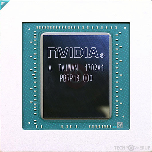
The Tesla P40 was an enthusiast-class professional graphics card by NVIDIA, launched on September 13th, 2016. Built on the 16 nm process, and based on the GP102 graphics processor, the card supports DirectX 12. The GP102 graphics processor is a large chip with a die area of 471 mm² and 11,800 million transistors. It features 3840 shading units, 240 texture mapping units, and 96 ROPs. NVIDIA has paired 24 GB GDDR5 memory with the Tesla P40, which are connected using a 384-bit memory interface. The GPU is operating at a frequency of 1303 MHz, which can be boosted up to 1531 MHz, memory is running at 1808 MHz (7.2 Gbps effective).
Being a dual-slot card, the NVIDIA Tesla P40 draws power from an 8-pin EPS power connector, with power draw rated at 250 W maximum. This device has no display connectivity, as it is not designed to have monitors connected to it. Tesla P40 is connected to the rest of the system using a PCI-Express 3.0 x16 interface. The card measures 267 mm in length, 111 mm in width, and features a dual-slot cooling solution. Its price at launch was 5699 US Dollars.
Being a dual-slot card, the NVIDIA Tesla P40 draws power from an 8-pin EPS power connector, with power draw rated at 250 W maximum. This device has no display connectivity, as it is not designed to have monitors connected to it. Tesla P40 is connected to the rest of the system using a PCI-Express 3.0 x16 interface. The card measures 267 mm in length, 111 mm in width, and features a dual-slot cooling solution. Its price at launch was 5699 US Dollars.
Graphics Processor
Graphics Card
- Release Date
- Sep 13th, 2016
- Generation
-
Tesla Pascal
(Pxx)
- Predecessor
- Tesla Maxwell
- Successor
- Tesla Volta
- Production
- End-of-life
- Launch Price
- 5,699 USD
- Bus Interface
- PCIe 3.0 x16
Relative Performance
Based on TPU review data: "Performance Summary" at 1920x1080, 4K for 2080 Ti and faster.
Performance estimated based on architecture, shader count and clocks.
Clock Speeds
- Base Clock
- 1303 MHz
- Boost Clock
- 1531 MHz
- Memory Clock
-
1808 MHz
7.2 Gbps effective
Memory
- Memory Size
- 24 GB
- Memory Type
- GDDR5
- Memory Bus
- 384 bit
- Bandwidth
- 347.1 GB/s
Render Config
- Shading Units
- 3840
- TMUs
- 240
- ROPs
- 96
- SM Count
- 30
- L1 Cache
- 48 KB (per SM)
- L2 Cache
- 3 MB
Theoretical Performance
- Pixel Rate
- 147.0 GPixel/s
- Texture Rate
- 367.4 GTexel/s
- FP16 (half)
- 183.7 GFLOPS (1:64)
- FP32 (float)
- 11.76 TFLOPS
- FP64 (double)
- 367.4 GFLOPS (1:32)
Board Design
- Slot Width
- Dual-slot
- Length
- 267 mm
10.5 inches
- Width
- 111 mm
4.4 inches
- TDP
- 250 W
- Suggested PSU
- 600 W
- Outputs
- No outputs
- Power Connectors
- 8-pin EPS
- Board Number
- PG610 SKU 200
Graphics Features
- DirectX
- 12 (12_1)
- OpenGL
- 4.6
- OpenCL
- 3.0
- Vulkan
- 1.3
- CUDA
- 6.1
- Shader Model
- 6.7
GP102 GPU Notes
| NVENC: 6th Gen NVDEC: 3rd Gen PureVideo HD: VP8 VDPAU: Feature Set H |
May 13th, 2024 04:22 EDT
change timezone
Latest GPU Drivers
New Forum Posts
- Looking for a new case, cube shaped only. (5)
- PSU Option for my PC (11)
- Purchased an AX1200i PSU as part of some forward planning, what tier is this PSU? (59)
- LOL ASUS says this is $200 in repair, Steve from gamers Nexus smokes ASUS, Steam Deck til I die boys!!!! (77)
- Cyberpunk 2077 Game Discussion (2126)
- AIO Water Cooler vs Tower Air Cooler (8)
- Which RAM for AMD 7950X3D (3)
- Soundbar or 2.1 speaker for virtual 3d audio in PC games... (12)
- How to optimize my PC by overclocking my system (11)
- Ryzen Owners Zen Garden (7308)
Popular Reviews
- ZMF Caldera Closed Planar Magnetic Headphones Review
- Corsair MP700 Pro SE 4 TB Review
- Bykski CPU-XPR-C-I CPU Water Block Review - Amazing Value!
- ThundeRobot ML903 NearLink Review
- Upcoming Hardware Launches 2023 (Updated Feb 2024)
- CHERRY XTRFY M64 Pro Review
- AMD Ryzen 7 7800X3D Review - The Best Gaming CPU
- ASUS Radeon RX 7900 GRE TUF OC Review
- Corsair iCUE Link RX120 RGB 120 mm Fan Review
- Sapphire Radeon RX 7900 GRE Pulse Review
Controversial News Posts
- Intel Statement on Stability Issues: "Motherboard Makers to Blame" (266)
- AMD to Redesign Ray Tracing Hardware on RDNA 4 (224)
- Windows 11 Now Officially Adware as Microsoft Embeds Ads in the Start Menu (171)
- NVIDIA to Only Launch the Flagship GeForce RTX 5090 in 2024, Rest of the Series in 2025 (151)
- Sony PlayStation 5 Pro Specifications Confirmed, Console Arrives Before Holidays (119)
- AMD's RDNA 4 GPUs Could Stick with 18 Gbps GDDR6 Memory (114)
- AMD Hits Highest-Ever x86 CPU Market Share in Q1 2024 Across Desktop and Server (110)
- AMD Ryzen 9 7900X3D Now at a Mouth-watering $329 (104)