Report an Error


NVIDIA GP102
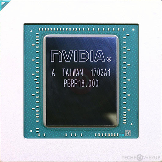
GP102

GP102-350-K1-A1

GP102-350-K2-A1

GP102-350-K3-A1

GP102-350-K4-A1

GP102-351-K1-A1

GP102-400-A1

GP102-450-A1

Fritzchens Fritz
Die Shot

Block Diagram

SM Diagram
NVIDIA's GP102 GPU uses the Pascal architecture and is made using a 16 nm production process at TSMC. With a die size of 471 mm² and a transistor count of 11,800 million it is a very big chip. GP102 supports DirectX 12 (Feature Level 12_1). For GPU compute applications, OpenCL version 3.0 and CUDA 6.1 can be used. It features 3840 shading units, 240 texture mapping units and 96 ROPs.
Graphics Processor
- Released
- Aug 2nd, 2016
- GPU Name
- GP102
- Codename
- NV132
- Architecture
- Pascal
- Foundry
- TSMC
- Process Size
- 16 nm
- Transistors
- 11,800 million
- Density
- 25.1M / mm²
- Die Size
- 471 mm²
- Package
- BGA-2397
Graphics Features
- DirectX
- 12 (12_1)
- OpenGL
- 4.6
- OpenCL
- 3.0
- Vulkan
- 1.3
- CUDA
- 6.1
- Shader Model
- 6.7
- WDDM
- 3.1
- NVENC
- 6th Gen
- NVDEC
- 3rd Gen
- PureVideo HD
- VP8
- VDPAU
- Feature Set H
Render Config
- Shading Units
- 3840
- TMUs
- 240
- ROPs
- 96
- SM Count
- 30
- SFUs
- 960
- TPCs
- 30
- GPCs
- 6
- L1 Cache
- 48 KB per SM
- L2 Cache
- 3072 KB
- Max. TDP
- 250 W
All Pascal GPUs
NVIDIA GPU Architecture History
- 2024 Blackwell
- 2023 Hopper
- 2022-2024 Ada Lovelace
- 2020-2024 Ampere
- 2018-2022 Turing
- 2017-2020 Volta
- 2016-2021 Pascal
- 2014-2019 Maxwell 2.0
- 2014-2017 Maxwell
- 2013-2015 Kepler 2.0
- 2012-2018 Kepler
- 2010-2016 Fermi 2.0
- 2010-2013 VLIW Vec4
- 2010-2016 Fermi
- 2007-2013 Tesla 2.0
- 2006-2010 Tesla
- 2003-2013 Curie
- 2003-2005 Rankine
- 2001-2003 Kelvin
- 1999-2005 Celsius
- 1998-2000 Fahrenheit
Graphics cards using the NVIDIA GP102 GPU
| Name | Chip | Memory | Shaders | TMUs | ROPs | Base Clock | Boost Clock | Memory Clock |
|---|---|---|---|---|---|---|---|---|
| GP102-400-A1 | 12 GB | 3584 | 224 | 96 | 1417 MHz | 1531 MHz | 1251 MHz | |
| GP102-875-A1 | 24 GB | 3840 | 240 | 96 | 1506 MHz | 1645 MHz | 1127 MHz | |
| GP102-350-K1-A1 | 11 GB | 3584 | 224 | 88 | 1481 MHz | 1582 MHz | 1376 MHz | |
| 24 GB | 3840 | 240 | 96 | 1303 MHz | 1531 MHz | 1808 MHz | ||
| GP102-450-A1 | 12 GB | 3840 | 240 | 96 | 1405 MHz | 1582 MHz | 1426 MHz | |
| GP102-100-A1 | 5 GB | 3200 | 200 | 80 | 1582 MHz | 1683 MHz | 1376 MHz | |
| GP102-101-A1 | 10 GB | 3200 | 200 | 80 | 1557 MHz | 1670 MHz | 2002 MHz | |
| 10 GB | 3200 | 200 | 80 | 1557 MHz | 1670 MHz | 1376 MHz | ||
| 24 GB | 3840 | 240 | 96 | 1025 MHz | 1493 MHz | 1808 MHz | ||
| 12 GB | 3200 | 200 | 80 | 1557 MHz | 1670 MHz | 1376 MHz |


GP102 GPU Notes
| NVENC: 6th Gen NVDEC: 3rd Gen PureVideo HD: VP8 VDPAU: Feature Set H |
Apr 27th, 2024 02:09 EDT
change timezone
Latest GPU Drivers
New Forum Posts
- What are you playing? (20541)
- What phone you use as your daily driver? And, a discussion of them. (1496)
- Safe memory overclock for the rtx 4050? (8)
- Help me identify rx 580 card ? (1)
- Your PC ATM (34511)
- RX 580 VBIOS related functionality not supported for Device: 0x67df (10)
- Strange system crashes out of nowhere, help (14)
- Alphacool CORE 1 CPU block - bulging with danger of splitting? (33)
- hacked (78)
- 5800x (and other Zen 3 chips) PBO settings/Temperature fix (937)
Popular Reviews
- Ugreen NASync DXP4800 Plus Review
- HYTE THICC Q60 240 mm AIO Review
- MOONDROP x Crinacle DUSK In-Ear Monitors Review - The Last 5%
- Upcoming Hardware Launches 2023 (Updated Feb 2024)
- Quick Look: MOONDROP CHU 2 Budget In-Ear Monitors
- Thermalright Phantom Spirit 120 EVO Review
- FiiO K19 Desktop DAC/Headphone Amplifier Review
- Alienware Pro Wireless Gaming Keyboard Review
- AMD Ryzen 7 7800X3D Review - The Best Gaming CPU
- Corsair iCUE Link XC7 RGB Elite CPU Water Block Review
Controversial News Posts
- Windows 11 Now Officially Adware as Microsoft Embeds Ads in the Start Menu (135)
- Sony PlayStation 5 Pro Specifications Confirmed, Console Arrives Before Holidays (117)
- NVIDIA Points Intel Raptor Lake CPU Users to Get Help from Intel Amid System Instability Issues (106)
- AMD "Strix Halo" Zen 5 Mobile Processor Pictured: Chiplet-based, Uses 256-bit LPDDR5X (103)
- US Government Wants Nuclear Plants to Offload AI Data Center Expansion (98)
- AMD's RDNA 4 GPUs Could Stick with 18 Gbps GDDR6 Memory (95)
- Developers of Outpost Infinity Siege Recommend Underclocking i9-13900K and i9-14900K for Stability on Machines with RTX 4090 (85)
- Windows 10 Security Updates to Cost $61 After 2025, $427 by 2028 (84)