Report an Error


NVIDIA Tesla P100 PCIe 12 GB
- Graphics Processor
- GP100
- Cores
- 3584
- TMUs
- 224
- ROPs
- 96
- Memory Size
- 12 GB
- Memory Type
- HBM2
- Bus Width
- 3072 bit

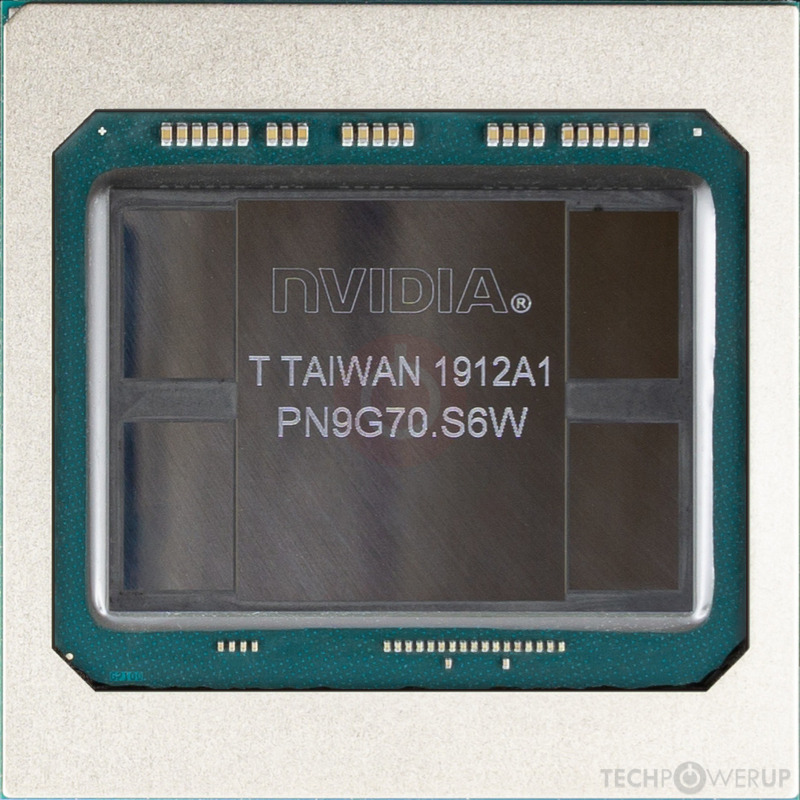
GPU
The Tesla P100 PCIe 12 GB was an enthusiast-class professional graphics card by NVIDIA, launched on June 20th, 2016. Built on the 16 nm process, and based on the GP100 graphics processor, in its GP100-892-A1 variant, the card supports DirectX 12. The GP100 graphics processor is a large chip with a die area of 610 mm² and 15,300 million transistors. It features 3584 shading units, 224 texture mapping units, and 96 ROPs. NVIDIA has paired 12 GB HBM2 memory with the Tesla P100 PCIe 12 GB, which are connected using a 3072-bit memory interface. The GPU is operating at a frequency of 1190 MHz, which can be boosted up to 1329 MHz, memory is running at 715 MHz.
Being a dual-slot card, the NVIDIA Tesla P100 PCIe 12 GB draws power from 1x 8-pin power connector, with power draw rated at 250 W maximum. This device has no display connectivity, as it is not designed to have monitors connected to it. Tesla P100 PCIe 12 GB is connected to the rest of the system using a PCI-Express 3.0 x16 interface. The card measures 267 mm in length, and features a dual-slot cooling solution. Its price at launch was 4599 US Dollars.
Being a dual-slot card, the NVIDIA Tesla P100 PCIe 12 GB draws power from 1x 8-pin power connector, with power draw rated at 250 W maximum. This device has no display connectivity, as it is not designed to have monitors connected to it. Tesla P100 PCIe 12 GB is connected to the rest of the system using a PCI-Express 3.0 x16 interface. The card measures 267 mm in length, and features a dual-slot cooling solution. Its price at launch was 4599 US Dollars.
Graphics Processor
Graphics Card
- Release Date
- Jun 20th, 2016
- Generation
-
Tesla Pascal
(Pxx)
- Predecessor
- Tesla Maxwell
- Successor
- Tesla Volta
- Production
- End-of-life
- Launch Price
- 4,599 USD
- Bus Interface
- PCIe 3.0 x16
Relative Performance
Based on TPU review data: "Performance Summary" at 1920x1080, 4K for RTX 3080 and faster.
Performance estimated based on architecture, shader count and clocks.
Clock Speeds
- Base Clock
- 1190 MHz
- Boost Clock
- 1329 MHz
- Memory Clock
-
715 MHz
1430 Mbps effective
Memory
- Memory Size
- 12 GB
- Memory Type
- HBM2
- Memory Bus
- 3072 bit
- Bandwidth
- 549.1 GB/s
Render Config
- Shading Units
- 3584
- TMUs
- 224
- ROPs
- 96
- SM Count
- 56
- L1 Cache
- 24 KB (per SM)
- L2 Cache
- 3 MB
Theoretical Performance
- Pixel Rate
- 127.6 GPixel/s
- Texture Rate
- 297.7 GTexel/s
- FP16 (half)
- 19.05 TFLOPS (2:1)
- FP32 (float)
- 9.526 TFLOPS
- FP64 (double)
- 4.763 TFLOPS (1:2)
Board Design
- Slot Width
- Dual-slot
- Length
- 267 mm
10.5 inches
- TDP
- 250 W
- Suggested PSU
- 600 W
- Outputs
- No outputs
- Power Connectors
- 1x 8-pin
Graphics Features
- DirectX
- 12 (12_1)
- OpenGL
- 4.6
- OpenCL
- 3.0
- Vulkan
- 1.3
- CUDA
- 6.0
- Shader Model
- 6.0
GP100 GPU Notes
| NVENC: 6th Gen NVDEC: 3rd Gen PureVideo HD: VP8 VDPAU: Feature Set H Latest Drivers: Windows 7 / 8 / 8.1 (x32 / x64): Quadro Release R390 U9 (392.37) / R440 U4 (441.66) Data Center Release 427.11 Windows 10 / 11 (x32 / x64): Quadro Release R390 U9 (392.37) / Latest Data Center Release: Latest |
Jul 25th, 2025 08:16 CDT
change timezone
Latest GPU Drivers
New Forum Posts
- R9 7900X - 5070Ti - Lags / Stuttering (32)
- Solidigm NVMe Custom Modded Driver for All NVMe Brands SSDs & Any NVMe SSDs (236)
- A Final Fantasy IX Reminiscence - My love letter and homage to one of the best stories ever told (127)
- AI Job Losses: let's count the losses up, total losses to AI so far 94,000 and counting (67)
- What's your latest tech purchase? (24364)
- TechPowerUp Screenshot Thread (MASSIVE 56K WARNING) (4278)
- How to get free Windows 10 security updates through October 2026: Two ways (11)
- Which Linux flavor? (58)
- DTS DCH Driver for Realtek HDA [DTS:X APO4 + DTS Interactive] (2233)
- Questionable quality future game releases being considered (3)
Popular Reviews
- Noctua NF-A12x25 G2 PWM Fan Review
- MSI MPG B850I Edge Ti Wi-Fi Review
- UPERFECT UMax 24 Review
- Cougar OmnyX Review
- TerraMaster F4-424 Max Review - The fastest NAS we've tested so far
- VAXEE XE V2 Wireless Review
- Sharkoon OfficePal C10 Review - Affordable and Decent
- Thermal Grizzly WireView Pro Review
- Upcoming Hardware Launches 2025 (Updated May 2025)
- Razer Blade 16 (2025) Review - Thin, Light, Punchy, and Efficient
TPU on YouTube
Controversial News Posts
- Some Intel Nova Lake CPUs Rumored to Challenge AMD's 3D V-Cache in Desktop Gaming (140)
- AMD Radeon RX 9070 XT Gains 9% Performance at 1440p with Latest Driver, Beats RTX 5070 Ti (131)
- AMD's Upcoming UDNA / RDNA 5 GPU Could Feature 96 CUs and 384-bit Memory Bus (121)
- NVIDIA GeForce RTX 5080 SUPER Could Feature 24 GB Memory, Increased Power Limits (115)
- NVIDIA DLSS Transformer Cuts VRAM Usage by 20% (99)
- AMD Sampling Next-Gen Ryzen Desktop "Medusa Ridge," Sees Incremental IPC Upgrade, New cIOD (97)
- NVIDIA Becomes First Company Ever to Hit $4 Trillion Market-Cap (94)
- Windows 12 Delayed as Microsoft Prepares Windows 11 25H2 Update (92)